This thread has been locked.

If you have a related question, please click the "Ask a related question" button in the top right corner. The newly created question will be automatically linked to this question.

how to wake up TPS65070 from sleep mode

Other Parts Discussed in Thread: TPS65070

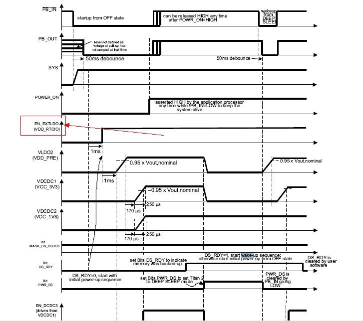
Could you please tell me how to wake up from sleep mode? Our customer have modification the TPS65070 EVM board  by connect the dcdc2 enable to dcdc2  output  to use the external enable function, at the time connect the Pgood to the DCDC1.

Now we find we can not wake up the unit from sleep mode. There is no response when we push the PB_in,  we also can not find the EN_EXTLDO in TPS65070, whats  the EN_EXTLDO use for?

  • How are you putting the device to sleep? When you pull PB_IN low, are you asserting POWER_ON pin high before releasing PB_IN? You said you have EN_DCDC2  tied to DCDC2 output, is that a typo?

    EXT_LDO is the same as VDD_RTC. It is named that way because it is tied to an external LDO as visible in the block diagram associated with the timing diagram you posted.

  • customer set the con_crtl2 bit 4 to 1 for the sleep mode.is it any problem here?

    for the EN_DCDC2, we just connect the EN_DCDC2 to DCDC2 outpt with a 10k resistor directely

    Could you please show the details to how to enter into the sleep mode and how to active it?

  • Could you please help answer below question?

    1. Power up

    How to set the start up sequence of DCDC1,DCDC2,DCDC3. we want to use the DCDC2 output 1.8v connect to Power_on to hold the Tps65070 when enter into the sleep mode.is there any problem here?


    2.sleep mode 

    We need the DCDC2 power on when enter into sleep mode. How to set the register and IO connection?


    3.if we want to wake up the sleep mode to normal mode,press the PB_in to low in order to power on DCDC1 and DCDC3, how to set the register?


    Yesterday I have test our TPS65070 EVM Board with customer and find that if we set the  CON_CTRL Bit 7:5 to 100 and CON_CTRL2 bit 5:3 to 110 with all the DCDC Enable IO pin to high,  then the TPS65070 will enter into sleep mode and only the DCDC2 is power on, press the PB_in can wake up all the DCDC output. This result is what we want ,however, I don’t understand the reason, it seems the result not match our datasheet. Could you please tell me why? I want know if there is any problem if we set the EVM like this in our real application.


    4.shut down

    Because we use the DCDC2 connect to Power_on to hold the TPS65070. can we use the I2C to shut down all the DCDC and LDO? If we can shut down all the output. Can we wake up the DCDC output by press the PB_IN?