Hello
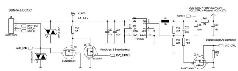
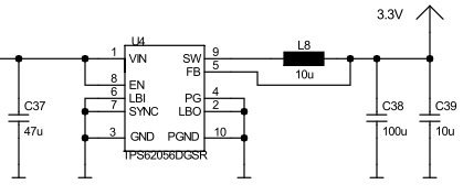
in an earlier revision we were using the TPS62056 (3.3V fixed output). Now we switched to the version with adjustable output TPS62050. We are using the switch converter with a external resistor divider. Using a FET driven by a micro controller one of the resistor values can be changed. So we are able to get 2.7 or 3.3V depending on the FET's state. (see schematics at the end)
The older revision did its work very fine.
The new boards with the configurable voltage appears to work fine as well - but we are getting big trouble:
The observations are:
- the output voltage often drops out
- and the TPS62050 gets very hot
- the circuit draws a lot of current without any load drawing it
- replacement of the TPS62050 on these boards with a new chip fixes the problem
- up to 20% of the boards have the problem just at the first power on after coming from production
- some of the boards are coming back from the field with the same problem after some time
So the question is: What is wrong with our boards. What did change to the first version what damages the chips? Ideas we have at the moment:
- the chips got damaged through production (soldering, moisture in package etc.)
- our idea to switch the resistor divider for getting 2 different output voltages is resulting in not allowed conditions to the TPS62050
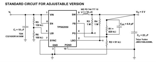
- the standard circuit (Datasheet page 15, Cff) uses a capacitor Cff with about 6.8pF we don't have in our schematic
Does anybody have any idea whats going wrong with our boards?
Schematics
Old fixed voltage version
New dual voltage version
(2.7 or 3.3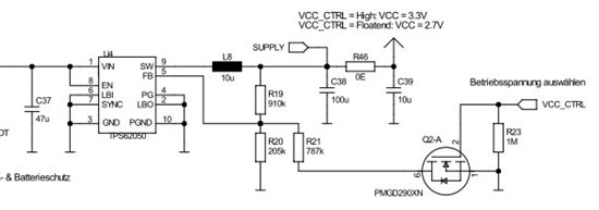 V)
V)
standard circuit (Datasheet page 15, Cff)