Tool/software:
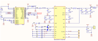
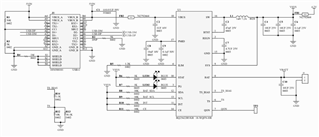
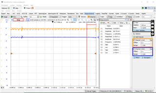
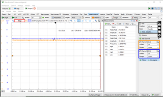
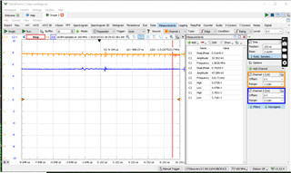
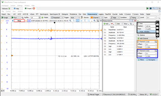
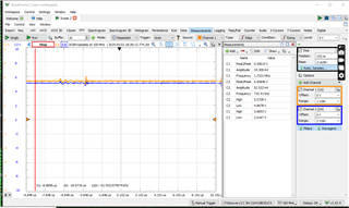
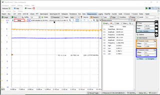
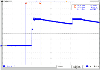
i attach the my design of BQ25622 , here when i connected the vbus to 5v source then BQ25622 ic will heated up too much ,help me to fixed this is this right design or i have to modified it if yes then provide suggestion
Tool/software:
i attach the my design of BQ25622 , here when i connected the vbus to 5v source then BQ25622 ic will heated up too much ,help me to fixed this is this right design or i have to modified it if yes then provide suggestion