This thread has been locked.

If you have a related question, please click the "Ask a related question" button in the top right corner. The newly created question will be automatically linked to this question.

LM51231-Q1: Loop Compensation and Bode Plot for LM51231-Q1 Boost Converter Design

Part Number: LM51231-Q1
Other Parts Discussed in Thread: LM5122

Tool/software:

Hi TI Team,

I am currently working on a boost converter design using the LM51231-Q1 with the following specifications:

  • Input Voltage: 12V

  • Output Voltage: 36V

  • Output Current: 12A

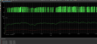
I found the TI Excel calculator for this design and have been following it, but I'm a bit confused about the loop compensation circuit and the bode plot. Specifically, the phase margin seems to be quite high, and I’m unsure if this is correct for the design.

Could someone help me understand if this specification is suitable for the LM51231-Q1, and whether a high phase margin is expected? I've attached the Excel sheet I’ve been working with for reference.

Any insights or suggestions would be greatly appreciated!

Thanks and Regards 

Vinod J 

0777.LM5123_Excel_Quickstart_Calculator_for_Boost_Controller_Design.xlsx

  • Hi Vinod,

    Thanks for using the e2e forum.
    The most important point within the phase graph is the value at the point of crossover frequency. This is the phase margin of your design.
    For you values, the calculators estimates a crossover frequency of ~2kHz (Gain crosses 0dB), and a phase margin of ~75°, which would be fully stable.
    Our general recommendation is to aim for 60° or more phase margin.

    I recommend to have a look at this app not for better understanding of the information you take take out of the bode diagram.
    https://www.ti.com/lit/an/slva381b/slva381b.pdf

    Please let me know if you have additional questions on this topic.

    Best regards,
    Niklas

  • Hi Niklas,

    Thanks for your response and for the detailed explanation.

    If I’m not mistaken, phase margin refers to the phase value at the gain crossover frequency — that is, the frequency where the gain crosses 0 dB. The phase margin is the difference between this phase value and -180°, correct?

    Appreciate the recommendation of the application note — I’ll go through it for a deeper understanding of the Bode plot analysis.

    Thanks again, and I’ll reach out if I have any further questions.

    Best regards,
    Vinod

  • Hi Vinod,

    You are correct.
    In the quickstart calculator, the phase curve is shifted by 180 degree to make it easier to read.
    I am sorry if this caused any confusion.

    Best regards,
    Niklas

  • Hi Niklas,

    I’ve now completed all the values and updated them accordingly. Could you please do a final review and let me know if everything looks good, so I can proceed with the design?

    Best regards,

    Vinod J 

     8308.LM5123_Excel_Quickstart_Calculator_for_Boost_Controller_Design.xlsx

  • Hi Vinod,

    Thanks for the filled in calculator.
    The gain curve of the bode plot seems to bounce back above the 0dB threshold, which is bad.
    Here I would derive a bit from the recommended compensation values and increase the Chf cap. (e.g. if you increase it to 500pF, the bode plot looks much better)
    The final stability of the design should be tested on bench, so you can still fine tune the compensation values later on.

    A general point I noticed is that you want to build a 430W application with just one phase.
    This is possible, but you layout and external components (MOSFETs/inductor) need to be able to support these current ratings.
    As seen by the calculator, the peak inductor current is 45A. You can use several MOSFETs in parallel to share the current, but you still have to consider that thermal behavior will be a challenge.

    An alternative solution would be to use a dual phase design with LM5122.

    Best regards,
    Niklas

  • Hi Niklas,

    Thanks for your reply and the helpful insights.

    I’ve updated the Chf capacitor to 500 pF as you suggested, and the Bode plot does look much better now. However, I noticed that in the simulation, the SW pin is not switching continuously after this change. For reference, the calculator originally recommended a Chf value of 34 pF, so this deviation might be affecting the loop behavior. I’ve attached an image of the simulation for your review.

    Regarding the power stage, I’m using the XGL1313-152MED inductor, which has a 53 A saturation current—this provides sufficient headroom. For the MOSFETs, I’ve selected four NTMFS5C670NLT1G devices (2 for high-side, 2 for low-side). These are rated at 60 V and 17 A (Ta), 71 A (Tc), and I believe they are suitable considering current sharing and thermal performance.

    Looking forward to your thoughts on the SW pin behavior.

    Best regards,

    Vinod J 

  • Hi Niklas, 

    I've been going through several discussions on the E2E forum and came across a few useful insights. One post mentioned that for a 200W power level, achieving efficiency and thermal management is relatively straightforward. However, when scaling beyond 400W, it becomes essential to use larger inductors and MOSFETs due to the increased current and switching losses.

    I wanted to get your feedback on the MOSFET and inductor parts I’ve currently selected for my design. Would you be able to review them and let me know if they are suitable for a power level above 400W? If not, I’d greatly appreciate your recommendations for alternate components that would be better suited for this power range.

    Additionally, another thread on the E2E forum mentioned the use of external gate drivers for the MOSFETs. Is it absolutely necessary to include a dedicated driver IC for driving these MOSFETs at higher power levels? If so, could you please suggest some recommended gate driver ICs that would be appropriate for this use case?

    And also I am operating LM51231-Q1 in 1MHz frequency and want to know how feasible it is using that MOSFET?

    Looking forward to your expert suggestions.

    Best regards,

    Vinod J 

  • Hi Vinod,

    Sorry for the long delay.

    Compensation:
    The final stability and compensation network should be fine tuned on bench, where all interferences are visible.
    But I agree with you that the switching already looks unstable in the simulation, which is a bad sign.
    A good approach to stabilize the circuit is by slowing down the loop response, e.g. select a lower bandwidth of 1kHz (or even lower), change the compensation network accordingly and see if the switching behavior looks more stable.

    Inductor/ MOSFET:
    Unfortunately, I am not an expert for inductor or MOSFET components, so I cannot say if these component are the best fit for these conditions, or if there is a better option. The internal drivers of the device are definitely strong enough to drive the MOSFETs, so implementing external drivers would be rather a question of whether efficiency can be increased this way.
    At these power levels, even at 98% efficiency, there are ~8.5W of losses that will heat up the board.

    Best regards,
    Niklas

  • Hi Niklas,

    Thanks a lot for your response.

    I completely agree that the compensation network should be tuned on the bench, and for that, we would need to measure the Bode plot. Typically, for Bode plot injection, we add a small resistor (around 20Ω to 100Ω) in the feedback path.
    I would appreciate your suggestion on where best to place this injection resistor — would it be better between REF/RANGE or between VOUT/SENSE?

    Also, based on some E2E forum discussions, I noted that achieving more than 200W output power while switching at 1MHz can lead to significant switching losses. Therefore, I have reduced the switching frequency to 440kHz to help manage efficiency and thermal performance.

    If you or your team could help review and confirm the selection of MOSFETs, inductors, and capacitors, it would be extremely helpful for us to move forward confidently.
    For thermal management, I am planning to use heatsinks on the PCB, especially at the MOSFET and inductor areas.

    Thanks again for your support!

    Best regards,

    Thanks and regards 

    Vinod J 

  • Hi Vinod,

    I would recommend to place the resistor for bode plot injection at the VOUT pin. In your case, the schematic already has the R7409 resistor for this.

    Higher switching frequency will increase the switching losses, but has a smaller inductor current ripple which reduces core losses. However, if the switching losses are dominating, it definitely makes sense to reduce the switching frequency, so I would agree with this change.

    Regarding the component selection, I would recommend to get in touch with the according manufacturers to find the most suitable parts, as these people should be able to give more valuable support on this than my team.
    For example, I know that coilcraft has a loss calculator for their inductors, where you can compare performance and losses of several inductors based on your design specs.

    Best regards,
    Niklas