This thread has been locked.

If you have a related question, please click the "Ask a related question" button in the top right corner. The newly created question will be automatically linked to this question.

TPS25751: Cannot flash to device from current configuration bug hardware device connected

Part Number: TPS25751
Other Parts Discussed in Thread: , BQ25756, BQ25792

Tool/software:

Hello,

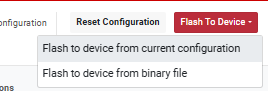
I'm currently using a TPS25751S to drive a USB 2.0 port in power source mode with associated data delivery. I have configured the various parameters required for the configuration on the GUI and connected my card to a USB port on the PC with the correct port and baud rate of 9600 (recommended) in the GUI settings. When I click on the banner at bottom left to connect my device, I manage to connect (little green button lit up). However, when I try to load the configuration on the card, it's impossible because it says “hardware is disconnected, try to refresh the page and reconnected hardware”.
Normally, I'm able to flash the code on my card. I use a ftdi usb uart bridge connected to an ESP32.

Does “hardware not connected” refer to the PD controller or the microcontroller?
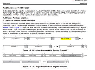
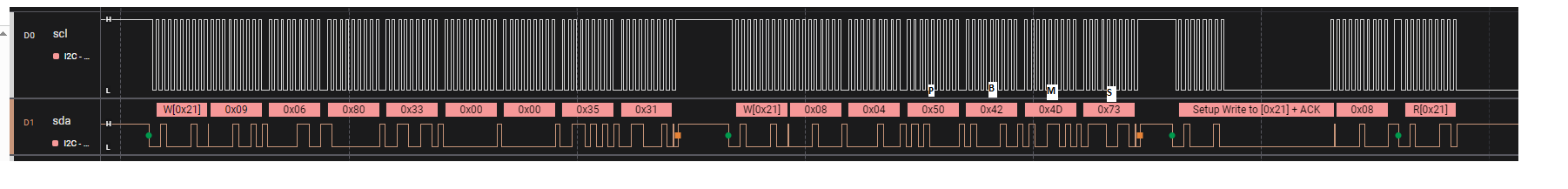
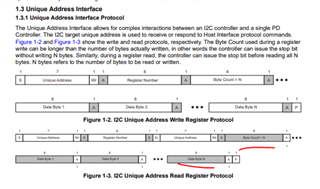
I ask this question because I use the I2Cc port for EEPROM + PD controller and I2Ct connected to the µC and PD controller. Unlike the EVM TPS25751D, I don't link the I2Ct bus between EEPROM and microcontroller.

I exported the LowRegionBinary and FullFlashBinary files in .C and flashed the config into the EEPROM from an external connector, so there's no design error on the EEPROM side.

Can you help me find a solution?

Best regards,

LEROY Corentin

  • Hi Leroy,

    I'm assuming you are talking about this?

    The Flash to Device option in the APP Config GUI is only meant for use with the TPS25751EVM.

    The connection status is looking for a TIVA mcu with proprietary FW on the USB port. It is not possible to use this setting without the EVM.

    For customer use, the expected usage is what you did in your second step.

    I exported the LowRegionBinary and FullFlashBinary files in .C and flashed the config into the EEPROM from an external connector, so there's no design error on the EEPROM side.

    We expect customers to use the Export Binary options paired with external programming of the EEPROM to program their systems.

    This is basically the same behavior as the Flash to Device button, we just use the Tiva to program the I2C EEPROM over the USB port.

    Thanks and Regards,

    Chris

  • Hello Chris,

    Sorry for the delay in responding. In fact I realised that flashing from the GUI is dedicated to the EVMs proposed by TEXAS. I have therefore generated a code that sends the I2C patches to the EEPROM or the PD controller and the patches are sent on the I2C buses. I can flash a patch to the controller but I can't get a PPS in source mode. Indeed, on the VBUS terminal (pin 26 and 27) I remain at 0V. I have +5V on PP5V (from a stable control system that can handle up to 3A). The source mode does not seem to be activated.

    I've followed the recommendations in the datasheet for routing the component, if you need the schematics I can share them with you.

    Currently on the PCB I'm not using Liquid Detection or BC and I'm on USB 2.0. I flash a patch generated on the GUI then exported without modifying any information in the ‘Advanced Configuration’ tab. How can I determine the source of the problem? Should I analyse the behaviour of the CC pins with an analyser?

    I've never used this type of component before and I don't have access to technical support in my team, so I'll take any advice/recommendations I can get.

    Thanks,

    LEROY Corentin

  • Hi Leroy,

    I can't get a PPS in source mode.

    What is a "PPS"?

    I'm assuming you are using the PBMx sequence to directly flash the PD controller over I2C?

    Are you sure you are flashing properly? Can you read registers from the PD controller? If so, I would recommend reading the MODE(0x03) register. If you have flashed the device properly, you should be able to read the register, decode the payload as ascii values, and it should read "APP ".

    Can you share the json you are using in the GUI to generate the binary and .c files?

    How can I determine the source of the problem? Should I analyse the behaviour of the CC pins with an analyser?

    We need to determine if it is flashing or config. You can first check the flashing portion by making sure the PD loads properly and checking MODE and Boot flags registers. See the TRM for more information on the registers.

    Analyzing the CC pins could help. If you are configured as source only and the PD controller is powered properly, you should see the CC pins pulled up to 3.3/5V.

    What type of sink device are you using? A USB-C PD sink, or Type-C only? When the sink is attached, you should see the CC lines settle at a voltage near 1.6-V.

    Thanks and Regards,

    Chris

  • What is a "PPS"?

    PPS is for Programmable Power Supply, from TPS25751 Datasheet.

    I do use the PBMx sequence from the Technical Reference Manuel for TPS25751 to directly flash into the PD controller. 

    Are you sure you are flashing properly? Can you read registers from the PD controller? If so, I would recommend reading the MODE(0x03) register. If you have flashed the device properly, you should be able to read the register, decode the payload as ascii values, and it should read "APP ".

    I first check with a i2c scan for the device to look at the address of the PD controller then process to send data but there might be something wrong with the functions i created. I'm still checking to see any error in code. I'm gonna check the MODE(0x03) register but cannot tell you until monday because of my schedule. 

    Can you share the json you are using in the GUI to generate the binary and .c files?

    Is there a tool to directly share files? I cannot use the Image/Video/File to import the .json and .c files 

    I don't want to copy/past the files content directly in the post.

    What type of sink device are you using? A USB-C PD sink, or Type-C only? When the sink is attached, you should see the CC lines settle at a voltage near 1.6-V.

    I am using a Android device like a tablet with a DRP rôle in it. I need to use the PD controller because with only RP or RD on CCx pins, I cannot manage to have both power source delivery from PCB and data delivery. I need to power the tablet while reading/writting data. 

    Thanks

    LEROY Corentin

  • Hi Leroy,

    You should be able to just drag and drop the files directly into the message box. Is there a reason you don't want to share the json directly into the post?

    I don't need the .C files, the json is enough.

    Can you share an I2C log of the PBMx process?

    Thanks and Regards,

    Chris

  • {
      "questionnaire": {
        "device": "TPS25751",
        "toolBuildVersion": "1.0.2",
        "answers": [
          null,
          8,
          4,
          4,
          0,
          1,
          3,
          0,
          1,
          0,
          1,
          null,
          0,
          0,
          0,
          0,
          0,
          0,
          0
        ],
        "vendorId": "4120",
        "productId": "0000",
        "version": "1.0.0.2"
      },
      "configuration": {
        "data": {
          "selected_ace": [
            {
              "register": 6,
              "data": [
                0,
                0,
                0,
                0,
                0,
                0,
                0,
                0
              ]
            },
            {
              "register": 22,
              "data": [
                0,
                0,
                0,
                0,
                0,
                0,
                0,
                0,
                0,
                0,
                3
              ]
            },
            {
              "register": 40,
              "data": [
                1,
                8,
                46,
                1,
                0,
                0,
                0,
                0,
                0,
                0,
                0,
                0,
                0,
                0,
                0,
                0,
                3
              ]
            },
            {
              "register": 41,
              "data": [
                194,
                80,
                129,
                0
              ]
            },
            {
              "register": 50,
              "data": [
                1,
                168,
                42,
                44,
                145,
                1,
                38,
                44,
                209,
                2,
                0,
                44,
                177,
                4,
                0,
                244,
                65,
                6,
                0,
                244,
                65,
                6,
                0,
                0,
                0,
                0,
                0,
                0,
                0,
                0,
                0,
                0,
                0,
                0,
                0,
                0,
                0,
                0,
                0,
                0,
                0,
                0,
                0,
                0,
                0,
                0,
                0,
                0,
                0,
                0,
                0,
                0,
                0,
                0,
                0,
                0,
                0,
                0,
                0,
                0,
                0,
                0,
                0
              ]
            },
            {
              "register": 51,
              "data": [
                0,
                44,
                145,
                1,
                16,
                44,
                209,
                2,
                0,
                44,
                177,
                4,
                0,
                244,
                65,
                6,
                0,
                69,
                65,
                6,
                0,
                0,
                0,
                0,
                0,
                0,
                0,
                0,
                0,
                0,
                0,
                0,
                0,
                0,
                0,
                0,
                0,
                0,
                0,
                0,
                0,
                0,
                0,
                0,
                0,
                0,
                0,
                0,
                0,
                0,
                0,
                0,
                0
              ]
            },
            {
              "register": 55,
              "data": [
                62,
                64,
                31,
                65,
                144,
                145,
                1,
                0,
                0,
                0,
                0,
                0,
                0,
                0,
                0,
                0,
                0,
                0,
                0,
                0,
                0,
                0,
                0,
                0
              ]
            },
            {
              "register": 66,
              "data": [
                26,
                0,
                8,
                0
              ]
            },
            {
              "register": 92,
              "data": [
                13,
                12,
                0,
                0,
                0,
                0,
                0,
                0,
                0,
                0,
                0,
                0,
                0,
                4,
                0,
                0,
                0,
                4,
                0,
                0,
                0,
                0,
                0,
                0,
                0,
                4,
                0,
                0,
                0,
                0,
                0,
                0,
                0,
                0,
                0,
                0,
                0,
                0,
                0,
                0,
                0,
                0,
                0,
                0,
                0,
                0,
                0,
                0,
                0
              ]
            },
            {
              "register": 112,
              "data": [
                3
              ]
            },
            {
              "register": 119,
              "data": [
                0,
                0,
                0,
                0,
                0,
                0,
                0,
                0,
                0,
                0,
                0,
                0,
                0,
                15,
                0
              ]
            },
            {
              "register": 122,
              "data": [
                0,
                0,
                0,
                0
              ]
            },
            {
              "register": 123,
              "data": [
                0,
                2,
                255,
                255,
                0,
                0,
                0,
                0,
                0,
                0,
                0,
                0,
                0,
                0,
                0,
                0
              ]
            },
            {
              "register": 125,
              "data": [
                0,
                0,
                0,
                0,
                0,
                0,
                0,
                0,
                0,
                0,
                0,
                0,
                0,
                0,
                0,
                0,
                0,
                0,
                0,
                0,
                0,
                0,
                0,
                0,
                0,
                0,
                0,
                0,
                0,
                0,
                0,
                0,
                0,
                0,
                0,
                0
              ]
            },
            {
              "register": 126,
              "data": [
                0,
                0,
                0,
                0,
                0,
                0,
                0,
                0,
                0,
                0,
                0,
                0,
                0,
                0
              ]
            },
            {
              "register": 152,
              "data": [
                0,
                0,
                0,
                0,
                0,
                0,
                0,
                0,
                0,
                0,
                0
              ]
            }
          ]
        }
      }
    }

    Hi Christopher,

    Sorry I couldn't share the json file in my previous reply, it seems this format isn't readable, I converted the file to .txt

    I'll share the I2C logs on Monday as I can't test this week due to my schedule. I'll get back to you on Monday.

    Kind regards,

    LEROY Corentin

  • Hi Leroy,

    Yeah, the txt file should work. I'm surprised you need to do that, typically I just drag and drop.

    {
      "questionnaire": {
        "device": "TPS25751",
        "toolBuildVersion": "1.0.2",
        "answers": [
          null,
          8,
          4,
          4,
          0,
          1,
          3,
          0,
          1,
          0,
          1,
          null,
          0,
          0,
          0,
          0,
          0,
          0,
          0
        ],
        "vendorId": "4120",
        "productId": "0000",
        "version": "1.0.0.2"
      },
      "configuration": {
        "data": {
          "selected_ace": [
            {
              "register": 6,
              "data": [
                0,
                0,
                0,
                0,
                0,
                0,
                0,
                0
              ]
            },
            {
              "register": 22,
              "data": [
                0,
                0,
                0,
                0,
                0,
                0,
                0,
                0,
                0,
                0,
                3
              ]
            },
            {
              "register": 40,
              "data": [
                1,
                8,
                46,
                1,
                0,
                0,
                0,
                0,
                0,
                0,
                0,
                0,
                0,
                0,
                0,
                0,
                3
              ]
            },
            {
              "register": 41,
              "data": [
                194,
                80,
                129,
                0
              ]
            },
            {
              "register": 50,
              "data": [
                1,
                168,
                42,
                44,
                145,
                1,
                38,
                44,
                209,
                2,
                0,
                44,
                177,
                4,
                0,
                244,
                65,
                6,
                0,
                244,
                65,
                6,
                0,
                0,
                0,
                0,
                0,
                0,
                0,
                0,
                0,
                0,
                0,
                0,
                0,
                0,
                0,
                0,
                0,
                0,
                0,
                0,
                0,
                0,
                0,
                0,
                0,
                0,
                0,
                0,
                0,
                0,
                0,
                0,
                0,
                0,
                0,
                0,
                0,
                0,
                0,
                0,
                0
              ]
            },
            {
              "register": 51,
              "data": [
                0,
                44,
                145,
                1,
                16,
                44,
                209,
                2,
                0,
                44,
                177,
                4,
                0,
                244,
                65,
                6,
                0,
                69,
                65,
                6,
                0,
                0,
                0,
                0,
                0,
                0,
                0,
                0,
                0,
                0,
                0,
                0,
                0,
                0,
                0,
                0,
                0,
                0,
                0,
                0,
                0,
                0,
                0,
                0,
                0,
                0,
                0,
                0,
                0,
                0,
                0,
                0,
                0
              ]
            },
            {
              "register": 55,
              "data": [
                62,
                64,
                31,
                65,
                144,
                145,
                1,
                0,
                0,
                0,
                0,
                0,
                0,
                0,
                0,
                0,
                0,
                0,
                0,
                0,
                0,
                0,
                0,
                0
              ]
            },
            {
              "register": 66,
              "data": [
                26,
                0,
                8,
                0
              ]
            },
            {
              "register": 92,
              "data": [
                13,
                12,
                0,
                0,
                0,
                0,
                0,
                0,
                0,
                0,
                0,
                0,
                0,
                4,
                0,
                0,
                0,
                4,
                0,
                0,
                0,
                0,
                0,
                0,
                0,
                4,
                0,
                0,
                0,
                0,
                0,
                0,
                0,
                0,
                0,
                0,
                0,
                0,
                0,
                0,
                0,
                0,
                0,
                0,
                0,
                0,
                0,
                0,
                0
              ]
            },
            {
              "register": 112,
              "data": [
                3
              ]
            },
            {
              "register": 119,
              "data": [
                0,
                0,
                0,
                0,
                0,
                0,
                0,
                0,
                0,
                0,
                0,
                0,
                0,
                15,
                0
              ]
            },
            {
              "register": 122,
              "data": [
                0,
                0,
                0,
                0
              ]
            },
            {
              "register": 123,
              "data": [
                0,
                2,
                255,
                255,
                0,
                0,
                0,
                0,
                0,
                0,
                0,
                0,
                0,
                0,
                0,
                0
              ]
            },
            {
              "register": 125,
              "data": [
                0,
                0,
                0,
                0,
                0,
                0,
                0,
                0,
                0,
                0,
                0,
                0,
                0,
                0,
                0,
                0,
                0,
                0,
                0,
                0,
                0,
                0,
                0,
                0,
                0,
                0,
                0,
                0,
                0,
                0,
                0,
                0,
                0,
                0,
                0,
                0
              ]
            },
            {
              "register": 126,
              "data": [
                0,
                0,
                0,
                0,
                0,
                0,
                0,
                0,
                0,
                0,
                0,
                0,
                0,
                0
              ]
            },
            {
              "register": 152,
              "data": [
                0,
                0,
                0,
                0,
                0,
                0,
                0,
                0,
                0,
                0,
                0
              ]
            }
          ]
        }
      }
    }

    I'll share the I2C logs on Monday as I can't test this week due to my schedule. I'll get back to you on Monday.

    Sounds good,

    Yeah try to get the PBMx I2C log and also check the Mode register. Those should help narrow down the problem.

    Thanks and Regards,

    Chris

  • Hi Christopher!

    I repeated the tests after updating my code, and the operating frequency of the I2C bus was too high (100k instead of 50k), which caused me to read errors on the bus.

    I can now view the contents of the MODE register (0X03) and it seems to remain 'stuck' in the PTC state:

    I (362) PD_CONFIG: Initializing I2C...
    I (372) PD_CONFIG: MODE Register: PTC
    I (372) PD_CONFIG: Sending PBMs command...
    I (472) PD_CONFIG: PBMs acknowledged: Patch burst mode started
    I (472) PD_CONFIG: MODE Register: PTC
    I (472) PD_CONFIG: Sending Low Region binary patch...
    I (33442) PD_CONFIG: Patch sent successfully!
    I (33442) PD_CONFIG: MODE Register: PTC
    I (33442) PD_CONFIG: Sending PBMc command...
    I (33542) PD_CONFIG: PBMc acknowledged: Patch burst mode completed
    I (33542) PD_CONFIG: Patch burst mode completed successfully!
    I (33542) PD_CONFIG: MODE Register: PTC
    I (33542) main_task: Returned from app_main()

    I checked the CC pins and they are at 0V even when the patch is loaded. I also have no power on the 27 and 26 pins (VBUS).

    I can share you the code if you want but what concernes me the most is why the register MODE is always in PTC.

    I can also tell that I am not doing a GO2P task after the PBMe because I have the Safemode activated on the PD controller (ADCINx pins tied to GND).

    I tried to increase the delay after a task to read the data in register MODE but this is always in PTC state. I can't read "APP" or "BOOT". 

    Do you want me to share the hardware schematic of the project so you can see on what kind of board I am working? Maybe I missunderstood something in the HW part (I use the S package of the TPS25751, not the D package)

    I'll update this message instead of creating others while continuing the tests to keep you updated.

    Do you advise me to create a new topic on the forum since the issue right now isn't related anymore to the first subject?

    KR,

    LEROY Corentin

  • Hi Leroy,

    This is still semi-related to your original issue, so it should be fine.

    A couple questions:

    1. How are you powering the system? Is VIN3V3 up and are the ADCIN and I2C pins "powered" properly. (i.e. pull up voltages active)
    2. I can't 100% tell from the log you shared, but your sequence for PBMx seems to look correct
      1. What do you mean by "PBMx acknowleged", what are you checking? Do you check that the CMD register is cleared? Are you reading the Data register and confirming no errors?
      2. For the patch bursts, how many bytes of Data are you sending each burst?
      3. For the PBMc command, do you read the output data in the data register? Could you report the value you read?
    3. Is the green unit ms?

    Here is a sample I2C log for a working PBMx flow on a similar device for reference. 

    PBMx_PowerUp_Two_994 (6).xlsx

    If possible, could you share something similar?

    Thanks and Regards,

    Chris

  • Hi Christophe,

    How are you powering the system? Is VIN3V3 up and are the ADCIN and I2C pins "powered" properly. (i.e. pull up voltages active)

    I am currently powering VIN3V3 with the output of a buck converter that also power my ESP32 and other modules on the PCB. I tied ADCIN pins to GND through 100k resistors but I can also change this configuration to tie them to either 1.5V or 3.3V (3.3V for ADCIN1 and 1.5V for ADCIN2). For the I2C but, I connected to same signal of VIN3V3 to pull up resistors of 4.7K to each SDA and SCL signals. 

    I have the I2C adress (0x21) related to the decoding #2 from the datasheet in power "safemode) because of the states of the ADC pins.

    What do you mean by "PBMx acknowleged", what are you checking? Do you check that the CMD register is cleared? Are you reading the Data register and confirming no errors?

    The PBMc command was sent without I2C communication errors. I don't check if CMD register is cleared, do I need to do it?

    For the patch bursts, how many bytes of Data are you sending each burst?

    I send 16 bytes of data per burst for all PBMx tasks.

    For the PBMc command, do you read the output data in the data register? Could you report the value you read?

    I didn't read the output data before, I looked at the reference manuel but I couldn't find the size of the data register so I suggested it equal to 8bytes, here is the output data log from data register :

    I (33542) PD_CONFIG: DATAX Register: 0x00 0x00 0x00 0x00 0x00 0x00 0x00 0x00

    Is the green unit ms?

    The unit refers to the timestamp in milliseconds since the system was started. It takes around 30seconds to launch the patch after the PBMs task.

    I'll update the message for the I2C log file in csv format, keep you update chris.

    KR,

    LEROY Corentin

  • Hi Leroy,

    The PBMc command was sent without I2C communication errors. I don't check if CMD register is cleared, do I need to do it?

    For all of the 4CC commands, it is recommended to read the CMD register after a command is written to it.

    3 responses are expected:

    1. Read back the command (i.e. you wrote PBMc, and it reads PBMc)
      1. This means the command is still processing
    2. Read back ascii "!CMD". Means the command is inavlid
    3. Read back zeroes
      1. Command has executed and completed.

    For every 4CC command, we recommend reading the CMD register and waiting until it clears to ensure the command executed.


    Can you share the .c file with the binary you generated and tell me what you write to the Data Register for the PBMs command?

    Thanks and Regards,

    Chris

  • Hi Chistopher,

    So since last week I have been able to try different things about the TPS25751S and here are my conclusions.

    Regarding your advices, I tried to see whats inside the CMD register each time I send a command on the TPS and it always returns !CMD. I share you the logs I have so you can see what i have. The issue is in the patch or the way I send it because the TPS still stay in PTCH mode.

    I (354) PD_CONFIG: Initializing I2C...
    I (364) PD_CONFIG: MODE Register: PTCH
    I (364) PD_CONFIG: Sending PBMs command...
    I (374) PD_CONFIG: CMD Register: !CMD
    I (474) PD_CONFIG: PBMs acknowledged: Patch burst mode started
    I (474) PD_CONFIG: MODE Register: PTCH
    I (474) PD_CONFIG: Sending Low Region binary patch...
    I (484) PD_CONFIG: CMD Register: !CMD
    I (494) PD_CONFIG: CMD Register: !CMD
    I (504) PD_CONFIG: CMD Register: !CMD
    I (514) PD_CONFIG: CMD Register: !CMD
    I (524) PD_CONFIG: CMD Register: !CMD
    I (534) PD_CONFIG: CMD Register: !CMD
    I (544) PD_CONFIG: CMD Register: !CMD
    I (554) PD_CONFIG: CMD Register: !CMD
    I (564) PD_CONFIG: CMD Register: !CMD
    I (574) PD_CONFIG: CMD Register: !CMD
    I (584) PD_CONFIG: CMD Register: !CMD
    I (594) PD_CONFIG: CMD Register: !CMD
    I (604) PD_CONFIG: CMD Register: !CMD
    I (614) PD_CONFIG: CMD Register: !CMD
    I (624) PD_CONFIG: CMD Register: !CMD
    I (634) PD_CONFIG: CMD Register: !CMD
    I (644) PD_CONFIG: CMD Register: !CMD
    I (654) PD_CONFIG: CMD Register: !CMD
    I (664) PD_CONFIG: CMD Register: !CMD
    I (674) PD_CONFIG: CMD Register: !CMD
    I (684) PD_CONFIG: CMD Register: !CMD
    I (694) PD_CONFIG: CMD Register: !CMD
    I (704) PD_CONFIG: CMD Register: !CMD
    I (714) PD_CONFIG: CMD Register: !CMD
    I (724) PD_CONFIG: CMD Register: !CMD
    I (734) PD_CONFIG: CMD Register: !CMD
    I (744) PD_CONFIG: CMD Register: !CMD
    I (754) PD_CONFIG: CMD Register: !CMD
    I (764) PD_CONFIG: CMD Register: !CMD
    I (774) PD_CONFIG: CMD Register: !CMD
    I (784) PD_CONFIG: CMD Register: !CMD
    I (794) PD_CONFIG: CMD Register: !CMD
    I (804) PD_CONFIG: CMD Register: !CMD
    I (814) PD_CONFIG: CMD Register: !CMD
    I (824) PD_CONFIG: CMD Register: !CMD
    I (834) PD_CONFIG: CMD Register: !CMD
    I (844) PD_CONFIG: CMD Register: !CMD
    I (854) PD_CONFIG: CMD Register: !CMD
    I (864) PD_CONFIG: CMD Register: !CMD
    I (874) PD_CONFIG: CMD Register: !CMD
    I (884) PD_CONFIG: CMD Register: !CMD
    I (894) PD_CONFIG: CMD Register: !CMD
    I (904) PD_CONFIG: CMD Register: !CMD
    I (914) PD_CONFIG: CMD Register: !CMD
    I (924) PD_CONFIG: CMD Register: !CMD
    I (934) PD_CONFIG: CMD Register: !CMD
    I (944) PD_CONFIG: CMD Register: !CMD
    I (954) PD_CONFIG: CMD Register: !CMD
    I (964) PD_CONFIG: CMD Register: !CMD
    I (974) PD_CONFIG: CMD Register: !CMD
    I (984) PD_CONFIG: CMD Register: !CMD
    I (994) PD_CONFIG: CMD Register: !CMD
    I (1004) PD_CONFIG: CMD Register: !CMD
    I (1014) PD_CONFIG: CMD Register: !CMD
    I (1024) PD_CONFIG: CMD Register: !CMD
    I (1034) PD_CONFIG: CMD Register: !CMD
    I (1044) PD_CONFIG: CMD Register: !CMD
    I (1054) PD_CONFIG: CMD Register: !CMD
    I (1064) PD_CONFIG: CMD Register: !CMD
    I (1074) PD_CONFIG: CMD Register: !CMD
    I (1084) PD_CONFIG: CMD Register: !CMD
    I (1094) PD_CONFIG: CMD Register: !CMD
    I (1104) PD_CONFIG: CMD Register: !CMD
    I (1114) PD_CONFIG: CMD Register: !CMD
    I (1124) PD_CONFIG: CMD Register: !CMD
    I (1134) PD_CONFIG: CMD Register: !CMD
    I (1144) PD_CONFIG: CMD Register: !CMD
    I (1154) PD_CONFIG: CMD Register: !CMD
    I (1164) PD_CONFIG: CMD Register: !CMD
    I (1174) PD_CONFIG: CMD Register: !CMD
    I (1184) PD_CONFIG: CMD Register: !CMD
    I (1194) PD_CONFIG: CMD Register: !CMD
    I (1204) PD_CONFIG: CMD Register: !CMD
    I (1214) PD_CONFIG: CMD Register: !CMD
    I (1224) PD_CONFIG: CMD Register: !CMD
    I (1234) PD_CONFIG: CMD Register: !CMD
    I (1244) PD_CONFIG: CMD Register: !CMD
    I (1254) PD_CONFIG: CMD Register: !CMD
    I (1264) PD_CONFIG: CMD Register: !CMD
    I (1274) PD_CONFIG: CMD Register: !CMD
    I (1284) PD_CONFIG: CMD Register: !CMD
    I (1294) PD_CONFIG: CMD Register: !CMD
    I (1304) PD_CONFIG: CMD Register: !CMD
    ...
    

    Here is the .c file where I'm doing the PBMs, PBMc , patch send, PBMe : 

    #include <stdio.h>
    #include "driver/i2c.h"
    #include "esp_log.h"
    #include "freertos/FreeRTOS.h"
    #include "freertos/task.h"
    #include "fullflash.h" // Contient le tableau tps25750x_lowRegion_i2c_array et gSizeLowRegionArray
    
    #define I2C_MASTER_SCL_IO    25
    #define I2C_MASTER_SDA_IO    26
    #define I2C_MASTER_NUM       I2C_NUM_0
    #define I2C_MASTER_FREQ_HZ   50000  // Réduisez la fréquence à 50 kHz
    #define I2C_MASTER_TX_BUF_DISABLE 0
    #define I2C_MASTER_RX_BUF_DISABLE 0
    
    #define PD_CTRL_ADDR         0x21  // Adresse principale du contrôleur PD
    #define PD_PATCH_ADDR        0x21  // Adresse utilisée pour la phase Burst Mode (vue avec I2C Scanner)
    #define REG_CMD              0x08  // Registre pour envoyer les commandes
    #define REG_STATUS           0x1A  // Registre de retour de statut
    #define REG_DATAX            0x09  // Registre pour lire les données de sortie
    #define TIMEOUT_MS           5000  // Augmentez le délai d'attente à 5 secondes
    
    static const char *TAG = "PD_CONFIG";
    
    static esp_err_t i2c_master_init(void) {
        i2c_config_t conf = {
            .mode = I2C_MODE_MASTER,
            .sda_io_num = I2C_MASTER_SDA_IO,
            .scl_io_num = I2C_MASTER_SCL_IO,
            .sda_pullup_en = GPIO_PULLUP_ENABLE,
            .scl_pullup_en = GPIO_PULLUP_ENABLE,
            .master.clk_speed = I2C_MASTER_FREQ_HZ,
        };
        esp_err_t ret = i2c_param_config(I2C_MASTER_NUM, &conf);
        if (ret != ESP_OK) {
            ESP_LOGE(TAG, "I2C param config failed: %s", esp_err_to_name(ret));
            return ret;
        }
        ret = i2c_driver_install(I2C_MASTER_NUM, conf.mode, I2C_MASTER_RX_BUF_DISABLE, I2C_MASTER_TX_BUF_DISABLE, 0);
        if (ret != ESP_OK) {
            ESP_LOGE(TAG, "I2C driver install failed: %s", esp_err_to_name(ret));
        }
        return ret;
    }
    
    static void log_i2c_write(uint8_t addr, uint8_t reg, const uint8_t *data, size_t len) {
        int64_t timestamp_us = 0;
        printf("%lld,WRITE,0x%02X,0x%02X", timestamp_us, addr, reg);
        for (size_t i = 0; i < len; ++i) {
            printf(",0x%02X", data[i]);
        }
        printf("\n");
    }
    
    static esp_err_t write_i2c(uint8_t addr, uint8_t reg, const uint8_t *data, size_t len) {
        i2c_cmd_handle_t cmd = i2c_cmd_link_create();
        i2c_master_start(cmd);
        i2c_master_write_byte(cmd, (addr << 1) | I2C_MASTER_WRITE, true);
        i2c_master_write_byte(cmd, reg, true);
        i2c_master_write(cmd, data, len, true);
        i2c_master_stop(cmd);
        esp_err_t ret = i2c_master_cmd_begin(I2C_MASTER_NUM, cmd, TIMEOUT_MS / portTICK_PERIOD_MS);
        // log_i2c_write(addr, reg, data, len);
        i2c_cmd_link_delete(cmd);
        if (ret != ESP_OK) {
            ESP_LOGE(TAG, "Failed to write to I2C address 0x%02X, reg 0x%02X: %s", addr, reg, esp_err_to_name(ret));
        }
        return ret;
    }
    
    static void log_i2c_read(uint8_t addr, uint8_t reg, const uint8_t *data, size_t len) {
        int64_t timestamp_us = 0;
        printf("%lld,READ,0x%02X,0x%02X", timestamp_us, addr, reg);
        for (size_t i = 0; i < len; ++i) {
            printf(",0x%02X", data[i]);
        }
        printf("\n");
    }
    
    static esp_err_t read_i2c(uint8_t addr, uint8_t reg, uint8_t *data, size_t len) {
        i2c_cmd_handle_t cmd = i2c_cmd_link_create();
        i2c_master_start(cmd);
        i2c_master_write_byte(cmd, (addr << 1) | I2C_MASTER_WRITE, true);
        i2c_master_write_byte(cmd, reg, true);
        i2c_master_start(cmd);  // Repeated start
        i2c_master_write_byte(cmd, (addr << 1) | I2C_MASTER_READ, true);
        i2c_master_read(cmd, data, len, I2C_MASTER_LAST_NACK);
        i2c_master_stop(cmd);
        esp_err_t ret = i2c_master_cmd_begin(I2C_MASTER_NUM, cmd, TIMEOUT_MS / portTICK_PERIOD_MS);
        // if (ret == ESP_OK) {
        //     log_i2c_read(addr, reg, data, len);
        // }
        i2c_cmd_link_delete(cmd);
        if (ret != ESP_OK) {
            ESP_LOGE(TAG, "Failed to read from I2C address 0x%02X, reg 0x%02X: %s", addr, reg, esp_err_to_name(ret));
        }
        return ret;
    }
    
    static void read_cmd_register() {
        uint8_t cmd[5] = {0};
        esp_err_t ret = read_i2c(PD_CTRL_ADDR, REG_CMD, cmd, 5);
        if (ret == ESP_OK) {
            ESP_LOGI(TAG, "CMD Register: %c%c%c%c%c", cmd[0], cmd[1], cmd[2], cmd[3], cmd[4]);
        } else {
            ESP_LOGE(TAG, "Failed to read CMD register: %s", esp_err_to_name(ret));
        }
    }
    
    void read_mode_register() {
        uint8_t mode[4] = {0};
        esp_err_t ret = read_i2c(PD_CTRL_ADDR, 0x03, mode, 5);
        if (ret == ESP_OK) {
            ESP_LOGI(TAG, "MODE Register: %c%c%c%c%c", mode[0], mode[1], mode[2], mode[3], mode[4]);
        } else {
            ESP_LOGE(TAG, "Failed to read MODE register: %s", esp_err_to_name(ret));
        }
    }
    
    static esp_err_t send_pbms_command(size_t bundle_size_bytes) {
        uint8_t pbms_data[7];
    
        // Taille du bundle en little-endian
        pbms_data[0] = bundle_size_bytes & 0xFF;        // Byte 1: bits 7:0
        pbms_data[1] = (bundle_size_bytes >> 8) & 0xFF;  // Byte 2: bits 15:8
        pbms_data[2] = (bundle_size_bytes >> 16) & 0xFF; // Byte 3: bits 23:16
        pbms_data[3] = (bundle_size_bytes >> 24) & 0xFF; // Byte 4: bits 31:24
    
        // Adresse cible I2C (7 bits valides seulement)
        // Byte 5: bits 6:0 pour l'adresse I2C cible, bit 7 réservé
        pbms_data[4] = PD_PATCH_ADDR & 0x7F;
    
        // Timeout recommandé = 0x32 (5s)
        // Byte 6: bits 5:0 pour la valeur de timeout, bits 7:6 réservés
        pbms_data[5] = 0x32;
    
        // Byte 7: réservé
        pbms_data[6] = 0x00;
    
        // Envoi des données via I2C
        esp_err_t ret = write_i2c(PD_CTRL_ADDR, REG_CMD, pbms_data, sizeof(pbms_data));
        if (ret != ESP_OK) {
            ESP_LOGE(TAG, "Failed to send PBMs command");
            return ret;
        }
    
        // Lire le registre CMD
        read_cmd_register();
    
        // Attente de statut de démarrage
        uint8_t status = 0xFF;
        for (int retries = 0; retries < 10; retries++) {
            vTaskDelay(100 / portTICK_PERIOD_MS);
            ret = read_i2c(PD_CTRL_ADDR, REG_STATUS, &status, 1);
            if (ret == ESP_OK) {
                if (status == 0x00) {
                    ESP_LOGI(TAG, "PBMs acknowledged: Patch burst mode started");
                    return ESP_OK;
                } else {
                    // Gestion des erreurs spécifiques
                    switch (status) {
                        case 0x04:
                            ESP_LOGE(TAG, "PBMs error: Invalid bundle size");
                            break;
                        case 0x05:
                            ESP_LOGE(TAG, "PBMs error: Invalid target address");
                            break;
                        case 0x06:
                            ESP_LOGE(TAG, "PBMs error: Invalid Timeout value");
                            break;
                        default:
                            ESP_LOGE(TAG, "PBMs unknown error status: 0x%02X", status);
                            break;
                    }
                    return ESP_FAIL;
                }
            }
        }
    
        ESP_LOGE(TAG, "Timeout waiting for PBMs ACK");
        return ESP_FAIL;
    }
    
    static esp_err_t send_patch_data(const uint8_t *data, size_t size) {
        for (size_t i = 0; i < size; i += 16) {
            size_t chunk_size = (i + 16 <= size) ? 16 : size - i;
            esp_err_t ret = write_i2c(PD_PATCH_ADDR, REG_CMD, &data[i], chunk_size);
            if (ret != ESP_OK) {
                ESP_LOGE(TAG, "Failed to send patch chunk at offset 0x%04X", (unsigned)i);
                return ret;
            }
            read_cmd_register();
            vTaskDelay(10 / portTICK_PERIOD_MS);
        }
        return ESP_OK;
    }
    
    static esp_err_t send_pbmc_command() {
        uint8_t pbmc_data[1] = {0x00}; // Pas de données d'entrée requises
    
        // Vérifier le registre MODE avant d'envoyer la commande PBMc
        uint8_t mode[4] = {0};
        esp_err_t ret = read_i2c(PD_CTRL_ADDR, 0x03, mode, 4);
        if (ret != ESP_OK) {
            ESP_LOGE(TAG, "Failed to read MODE register: %s", esp_err_to_name(ret));
            return ret;
        }
        if (mode[0] == 'A' && mode[1] == 'P' && mode[2] == 'P' && mode[3] == ' ') {
            ESP_LOGE(TAG, "PD controller is in APP mode, rejecting PBMc command");
            return ESP_FAIL;
        }
    
        ret = write_i2c(PD_CTRL_ADDR, REG_CMD, pbmc_data, sizeof(pbmc_data));
        if (ret != ESP_OK) {
            ESP_LOGE(TAG, "Failed to send PBMc command");
            return ret;
        }
    
        // Lire le registre CMD
        read_cmd_register();
    
        // Attente de statut de complétion
        uint8_t status[2] = {0xFF, 0xFF};
        for (int retries = 0; retries < 10; retries++) {
            vTaskDelay(100 / portTICK_PERIOD_MS);
            ret = read_i2c(PD_CTRL_ADDR, REG_STATUS, status, 2);
            if (ret == ESP_OK) {
                if (status[0] == 0x00 && status[1] == 0x00) {
                    ESP_LOGI(TAG, "PBMc acknowledged: Patch burst mode completed");
    
                    // Read the output data from the DATAX register
                    uint8_t datax[8] = {0}; // Assuming DATAX is 8 bytes long
                    ret = read_i2c(PD_CTRL_ADDR, REG_DATAX, datax, sizeof(datax));
                    if (ret == ESP_OK) {
                        ESP_LOGI(TAG, "DATAX Register: 0x%02X 0x%02X 0x%02X 0x%02X 0x%02X 0x%02X 0x%02X 0x%02X",
                                 datax[0], datax[1], datax[2], datax[3], datax[4], datax[5], datax[6], datax[7]);
                    } else {
                        ESP_LOGE(TAG, "Failed to read DATAX register: %s", esp_err_to_name(ret));
                    }
    
                    return ESP_OK;
                } else {
                    // Gestion des erreurs spécifiques
                    ESP_LOGE(TAG, "PBMc error: DevicePatchCompleteStatus = 0x%02X, AppConfigPatchCompleteStatus = 0x%02X", status[0], status[1]);
                    return ESP_FAIL;
                }
            }
        }
    
        ESP_LOGE(TAG, "Timeout waiting for PBMc ACK");
        return ESP_FAIL;
    }
    
    static esp_err_t send_go2p_command() {
        uint8_t go2p_data[1] = {0x00}; // Pas de données d'entrée requises
    
        esp_err_t ret = write_i2c(PD_CTRL_ADDR, REG_CMD, go2p_data, sizeof(go2p_data));
        if (ret != ESP_OK) {
            ESP_LOGE(TAG, "Failed to send GO2P command");
            return ret;
        }
    
        // Lire le registre CMD
        read_cmd_register();
    
        // Attente de statut de complétion
        uint8_t status = 0xFF;
        for (int retries = 0; retries < 10; retries++) {
            vTaskDelay(100 / portTICK_PERIOD_MS);
            ret = read_i2c(PD_CTRL_ADDR, REG_STATUS, &status, 1);
            if (ret == ESP_OK) {
                if (status == 0x00) {
                    ESP_LOGI(TAG, "GO2P acknowledged: Entered patch mode");
                    return ESP_OK;
                } else {
                    // Gestion des erreurs spécifiques
                    ESP_LOGE(TAG, "GO2P error: Status = 0x%02X", status);
                    return ESP_FAIL;
                }
            }
        }
    
        ESP_LOGE(TAG, "Timeout waiting for GO2P ACK");
        return ESP_FAIL;
    }
    
    void app_main(void) {
        ESP_LOGI(TAG, "Initializing I2C...");
        ESP_ERROR_CHECK(i2c_master_init());
    
        // Lire le registre MODE avant de commencer
        read_mode_register();
    
        ESP_LOGI(TAG, "Sending PBMs command...");
        esp_err_t ret = send_pbms_command(gSizeLowRegionArray);
        if (ret != ESP_OK) {
            ESP_LOGE(TAG, "Failed to send Low Region config");
            return;
        }
    
        // Lire le registre MODE après avoir envoyé la commande PBMs
        read_mode_register();
    
        ESP_LOGI(TAG, "Sending Low Region binary patch...");
        ret = send_patch_data(tps25750x_lowRegion_i2c_array, gSizeLowRegionArray);
        if (ret == ESP_OK) {
            ESP_LOGI(TAG, "Patch sent successfully!");
        } else {
            ESP_LOGE(TAG, "Patch transmission failed!");
            return;
        }
    
        // Lire le registre MODE après avoir envoyé les données du patch
        read_mode_register();
    
        ESP_LOGI(TAG, "Sending PBMc command...");
        ret = send_pbmc_command();
        if (ret == ESP_OK) {
            ESP_LOGI(TAG, "Patch burst mode completed successfully!");
        } else {
            ESP_LOGE(TAG, "Failed to complete patch burst mode");
            return;
        }
    
        // Lire le registre MODE après avoir envoyé la commande PBMc
        read_mode_register();
    
        // Envoyer la commande GO2P pour forcer le passage en mode application
        // ESP_LOGI(TAG, "Sending GO2P command...");
        // ret = send_go2p_command();
        // if (ret == ESP_OK) {
        //     ESP_LOGI(TAG, "Entered patch mode successfully!");
        // } else {
        //     ESP_LOGE(TAG, "Failed to enter patch mode");
        //     return;
        // }
    
        // Lire le registre MODE après avoir envoyé la commande GO2P
        read_mode_register();
    }
    

    By binary do you want the one generated by Texas for the patch or the one of my project so you can try it?

    KR, 

    LEROY Corentin

  • Hi Leroy,

    By binary do you want the one generated by Texas for the patch or the one of my project so you can try it?

    Yeah, I was originally asking for the .c patch file, but not to try it.

    It seems like you are having a different issue, but a common issue we see is users not populating the PBMs data payload correctly, specifically seeing issues with the patch size field. Your issues appears to primarily be the !CMD so let's start there.

    Let's tackle the !CMD issue first

    How are you writing to the CMD registers? What does the payload look like?

    Here is a capture of a PBMs command that executes properly that you might be able to use as reference.

    Remember that the first payload byte is a "num bytes" and the 4CC command should be sent out left to right. (i.e., for PBMs, P is sent first)

    Thanks and Regards,

    Chris

  • Hi Christopher,

    I didn't had any logic analyser so I bought one and I can see the logic signals coming from the I2C bus. 

    Here is what I get when I run the code on Logic 2 regarding your example:

    The first one is the ascii format of the data send to the TPS with a !CMD at the end after what should be the "PBMS". I send you the hexa format so you can see I write on the 0X21 address of the device a patch of data : 

    How are you writing to the CMD registers? What does the payload look like?

    I write in the CMD registers using write_i2c(PD_CTRL_ADDR, REG_CMD, data, length); from a external example code I use as reference for the I2C protocol.

    You have an example of payload for the send of patch. I send a burst of 16 data packets for the patch, for PBMs I send  a burst of 7 data packets and for PBMc I send 1 data to end the transmission.

    I can't see the "PBMS" hexa data send to the TPS. It seems I don't send the the PBMs to the component. I'll update this message to let you know what I am doing.

    You can see at the end of the payload the "!CMD" encoded.

    I think I missed something. In the patch generated by Texas, Does it have the encoded "PBMs" directly in the tab? Also, what is the first logical trace sent before PBMS? It's not “DATA1” but I don't know what it is. As explained in the technical documentation, I need to send "DATA1" then 'PBMS" am i right?

    Kr

    LEROY Corentin

  • Hi Leroy,

    Thanks for the logs, this helps a lot!

    It seems like you are using the I2C interface and the "4CC" commands incorrectly.

    The TPS25751 uses SMBUS, which requires that the you send the register address, then the number of data bytes to write(Byte Count = N), then the data bytes.

    See the attached document for correct usage of the "4CC" commands. "PBMs" counts as a 4CC command.

    5824.Using 4CC Commands.pdf

    The "INPUT DATA" should be written to the Data register(0x09) first, and then the 4CC command "PBMs" should be written to the CMD(0x08) register.

    In the I2C log I shared, you can see the write to the Data register that occurs first.

    In this case, we are writing to register 0x09, there are "0x06" data bytes to be written, and 0x80 is the first byte of the "INPUT DATAX" payload. The bundle size (bytes 0-3) is 0x00 0x00 0x33 0x80, the I2C target is 0x35, and the timeout value is 0x31.

    Thanks and Regards,

    Chris

  • Hi Christopher,

    The last data packet sent seems to work for the PBMs task and sending the patch. This is what I was able to test at the end of the day yesterday.

    Here are the logs for the PBMs and for one example of 64bytes of data send to the TPS : 

    The second screen is after reading the command register to see the output data register.

    The second screen is the end of the send of 64 bytes of data, I can read the CMD register and there is no "!CMD" anymore.

    On the pdf you send me, it is recommanded to read the output data register after 

    I can't test it today, but I think I'll be able to tomorrow or the day after.

    Thanks for sharing the document, I wasn't actually sending "DATA1" before PBMs and, more importantly, I was sending "PBMS" and not "PBMs" at the start, my hex encoding was 0x53.

    I couldn't do so with the PBMc yesterday so I am going to modify the code to send the correct payload and read the mode register at the end .

    I'll keep you in touch, thanks a lot Christopher!

    Edit : I modified in my code the address of the I2C target, it was not correct (0x21 instead of 0x35) but on the measurements it doesn't seem to create any issue, I don't read the 0x05 data in output data register.So even if I set an address for I2C target that is wrong, it seems to work, am I wrong?

    KR,

    Leroy Corentin

  • Hi Leroy,

    If you are using a Saleae, feel free to send the .sal logs, I also have the Logic sw and can view the full log.

    On the pdf you send me, it is recommanded to read the output data register after 

    I can't test it today, but I think I'll be able to tomorrow or the day after.

    Sure. Yes, this is an important step to ensure that the command has executed and completed.


    I modified in my code the address of the I2C target, it was not correct (0x21 instead of 0x35) but on the measurements it doesn't seem to create any issue, I don't read the 0x05 data in output data register.So even if I set an address for I2C target that is wrong, it seems to work, am I wrong?

    I'm not entirely sure what you mean here (changing the address and 0x05 data)

    Regarding the device I2C address, for the 4CC commands and normal usage, the device I2C address is set by the ADCIN config.

    The EVM I use to test on has the device address set to 0x21(Index #2).

    The address of 0x35 is only used for the 64 byte burst and is set by the PBMs command. You should be able to use any value you want for this address, provided there are no other peripherals on the I2C bus that already use the address.

    Basically, for the Burst portion of the PBMx patching process, you can use any address you want, just make sure (1) you set it in PBMs, (2) it is used for the bursts and (3) it is not used by any other peripherals on the bus.

    Here is an example PBMx log taken with an EVM. There are some shortcuts taken (not reading full registers, not always checking if CMD register is cleared) but it should help with the overall flow of the process. You should primarily be interested in the traffic between 4-s and 6-s

    https://e2e.ti.com/cfs-file/__key/communityserver-discussions-components-files/196/PBMs.sal

    Thanks and Regards,

    Chris

  • Hi Christopher,

    So here is the saleae file if you want it  : 

    saleae_tp25751.zip

    The address of 0x35 is only used for the 64 byte burst and is set by the PBMs command. You should be able to use any value you want for this address, provided there are no other peripherals on the I2C bus that already use the address.

    Ok thanks, I keep the 0x35 so I respect the template you send me.

    Here is an example PBMx log taken with an EVM. There are some shortcuts taken (not reading full registers, not always checking if CMD register is cleared) but it should help with the overall flow of the process. You should primarily be interested in the traffic between 4-s and 6-s

    So I have a few questions regarding you example compared to mine. It seems your separe each payload of 64bytes by 1ms and I do it shortly. Can this be an issue if I am more around 200µs between each payload? Also, why is the CMD register taking so long to send the PBMc command on you example? Because you send PBMc and then you read multiple time de CMD register before it is free and then you manage to have the APP on the MODE register, but wait it is taking so long to free the CMD (around 300ms regarding your .sal file)?

    In my case I don't have to way too long before reading the CMD register empty but after sending PBMc I can't find the status register set to APP, it is always PTCH. I'll keep you in touch with that, I think the way I send the patch might be wrong, I defenetly don't have the same pattern as you.

    Edit : So i couldn't directly send you the .sal file, i putted it in the zipped folder at the beginning of the message so you can see my logs.

    KR 

    Leroy Corentin

  • Hi Leroy,

    It seems your separe each payload of 64bytes by 1ms and I do it shortly. Can this be an issue if I am more around 200µs between each payload?

    That's a limitation of the I2C Host we are using, 200us should be fine.

    Also, why is the CMD register taking so long to send the PBMc command on you example?

    We do recommend at least 500us between the end of the burst and the PBMc command. I'm not sure why the sample log we have waits 50ms, but I would recommend following the TRM. I'll check with the team to see if there was a specific reason and let you know if I hear anything.

    In my case I don't have to way too long before reading the CMD register empty but after sending PBMc I can't find the status register set to APP, it is always PTCH. I'll keep you in touch with that, I think the way I send the patch might be wrong, I defenetly don't have the same pattern as you.

    Read back the output data after the PBMc command, there may be info why it is failing in the response.

    Thanks and Regards,

    Chris

  • Hi Christopher,

    Read back the output data after the PBMc command, there may be info why it is failing in the response.

    So I was able to compare the byte values with those in the datasheet and here are my conclusions:

    Here is the data_output after loading the patch : 

    No patch is sent on TPS25751(configBundleGood is 0 but should be 1, acState is 0 but should be 0x07 and rpState is 0). I did set the I2C target address to 0x35 in CMD1, when sending DATA1 before PBMs, but I'm surprised to see that :
    DevicePatchCompleteStatus is 0
    AppConfigPatchCompleteStatus is also 0 (see screenshot).

    So there seems to be a “default” state for the data_output register and that's what I see in the document for the 4CC line you shared me few days ago : 

    "In many cases, the Output Data will return a “Standard Task Code”. The table referenced within the Output DataX section maps the value read from the register to each case in Output DataX. There is an example that navigates this case below."

    Does it mean I don't really see what's in data_output register? 

    I checked multiple times the register after loading the patch and it never change. I also did it at the beginning of the measurements, right after reading the CMD1 register with the "PBMs" send. And the data inside isn't exactly the same : 

    So here I have 0x40 0x00 instead of 0x40 0x03. 

    I send you the logs so you can see directly from you analyser. I can assure you I read all the low_region .c file generated by texas to load the patch. 

    Can the hardware cause any issue for the patch loading?

    Here are the logs : 

    saleae_multiple_read_data_output.zip

    As always, I'll keep you in touch by editing this message if I have anything new .

    Kind Regards

    LEROY Corentin

  • Hi Leroy,

    Not 100% sure if this is the only issue, but I took a quick look through your logs and noticed that you don't send the full PBMs command?

    This is near the 1.5s mark

    Also, immediately after, you are reading register 0x10? Did you mean to read 0x08 here?

    Thanks and Regards,

    Chris

  • Hi Christopher,

    Sorry I send you a log file that was not respecting the time delay between each write/read procedure, leading to false values for either data send (so 's' was not send corretcly) or data received. 

    Here is the new log file that shows the correct sequence of data and the patch load, then reading the CMD register with the same observation as before (refering to the former message in send you).

    0820.saleae_multiple_read_data_output.zip

    Also, I tried with the external EEPROM because I really wanted to see if this option could work and after generating the fullflash .c file, I send it following the page write sequence and the PD controller went into 'APP' mode, I read the MODE register after loading the patch in the EEPROM then repowered the PCB. 

    Unfortunately, the patch wasn't working, I tried to connect an android device to see if it can sink current from the PCB and if the data delivery is possible but nothing happened.

    I also tried to use the BC1.2 protocol instead of the USB-PD. I modified the patch by using the BC 1.2 in CDP mode (to enable the data delivery). I also configured GPIO4 and 5 to D+ and D- so I can respect the USB standard in terms of battery charge. Unfortunately this doesn't work either.

    On reading the datasheet, I noticed that I haven't integrated any components such as BQ25792 and BQ25756 as indicated:

    The TPS25751 supports Programmable Power Supply (PPS) source and sink. When the TPS25751 negotiates a PPS contract as a source, the device enables the high-voltage power path (PPHV for D variant, PPEXT for S variant) and communicate with the supported TI battery charger (BQ25792 and BQ25756) to supply the negotiated voltage

    Is this a major shortcoming in my use case if I try to use BC1.2 instead of USB-PD?

    Edit : I can try either BC1.2 or USB-PD because I don't want any power above 5V and 1.5Amps (500mA would be also ok) and I can achieve that with both, but not with the same pins).

  • Hello,

    Today is a TI US holiday.  Please excuse the delay.

    Regards

    Chris

  • Hi Leroy,

    When writing the "Bursts", they should be I2C writes to device address 0x35, not to 0x21. 

    This is the first burst you send out.

    First burst in example log I shared


    What are your port requirements?

    • Power roles
    • power level
    • Data roles
    • Data speeds

    Can you share your latest json?


    Also, I tried with the external EEPROM because I really wanted to see if this option could work and after generating the fullflash .c file, I send it following the page write sequence and the PD controller went into 'APP' mode, I read the MODE register after loading the patch in the EEPROM then repowered the PCB. 

    Unfortunately, the patch wasn't working, I tried to connect an android device to see if it can sink current from the PCB and if the data delivery is possible but nothing happened.

    It's good that the EEPROM loads into APP mode.

    It would be best to start with a basic 5V source only configuration for initial testing. Are you providing 5V to PP5V and PPHV?

    How do you intend provide voltage as a source? The PD controller is a switch, and needs at least a 5V rail connected to PP5V and a variable output DC-DC if wanting to support 5-20V.

    The TPS25751 supports Programmable Power Supply (PPS) source and sink. When the TPS25751 negotiates a PPS contract as a source, the device enables the high-voltage power path (PPHV for D variant, PPEXT for S variant) and communicate with the supported TI battery charger (BQ25792 and BQ25756) to supply the negotiated voltage

    Is this a major shortcoming in my use case if I try to use BC1.2 instead of USB-PD?

    You are somewhat correct here. PPS is a variable contract that consists of the sink regularly requesting updated Voltages and currents. In a PPS contract, the DC-DC supplying the sourcing power needs to be regularly updated, and this is typically supported through and I2C connection between the PD controller and the DC-DC, through which the contract voltage and current can be updated.

    We only natively support specific BQ devices, which are the ones listed in the gui.

    But PPS and BC1.2 are not the same same thing. BC1.2 is limited to 5-V and is non-PD and does not necessarily need a BQ device connected. You should be fine using BC1.2 without a BQ device, but there may be other reasons to have one if you need bidirectional power or voltages > 5-V.

    Edit : I can try either BC1.2 or USB-PD because I don't want any power above 5V and 1.5Amps (500mA would be also ok) and I can achieve that with both, but not with the same pins).

    If you are not looking to source more than 5V 1.5-A you should not support PPS. Type-C, Bc1.2, and USB-C PD @ 5-V/1.5-A should all be fine.

    Are you sure you need a PD controller? If you only need to supply Type-C 1.5-A you may be able to get away with a type-c port controller.

    Thanks and Regards,

    Chris

  • Hi Chistopher,

    It would be best to start with a basic 5V source only configuration for initial testing. Are you providing 5V to PP5V and PPHV?

    I provide 4.92V on PP5V and VSYS (because I have chose the S package).

    How do you intend provide voltage as a source? The PD controller is a switch, and needs at least a 5V rail connected to PP5V and a variable output DC-DC if wanting to support 5-20V.

    I have a stable PP5V input which, when the PPS source mode is activated, supplies +5V on pins 26 and 27 (VBUS) connected to the USB C port. For the current, I have a limit of 1.5A on my circuit, so I can stay on standard 5V 1.5A.

    But PPS and BC1.2 are not the same same thing. BC1.2 is limited to 5-V and is non-PD and does not necessarily need a BQ device connected. You should be fine using BC1.2 without a BQ device, but there may be other reasons to have one if you need bidirectional power or voltages > 5-V.

    I don't need a USB C port in DRP mode, just in DFP mode to power an android device while communicating data bi-directionally. It's important to have this bidirectional capability for data, because data exchanges are continuous.
    As I'm using an android device in DRP mode, which can normally support either the BC1.2 or USB-PD protocol, I can choose one or the other, but in the most logical case it's preferable to use a patch with USB-PD, but I wanted to test both, and as USB-PD didn't work, I tried to switch to BC1.2 by regenerating a patch.

    Are you sure you need a PD controller? If you only need to supply Type-C 1.5-A you may be able to get away with a type-c port controller.

    The problem, as I understand it, is that I need to power an external device and transmit data bidirectionally. This configuration is not native, from an HW configuration point of view, setting the CC pins to either pull up or pull down doesn't allow to negotiate both data transfer and load. A USB port controller might be a more suitable solution? The difference with a PD controller is the non-negotiation of the power supply direction? Knowing that the android device is in DRP, wouldn't it be a problem to set up a source power direction on my side and sink on the android device side?

    Kind Regards,

    LEROY Corentin

  • Hi Leroy,

    For 5-V Source only, you should be fine. Can you share the latest json you are using? I can review it to see if there is a reason why 5-V sourcing is not working.

    I don't need a USB C port in DRP mode, just in DFP mode to power an android device while communicating data bi-directionally. It's important to have this bidirectional capability for data, because data exchanges are continuous.

    If the port only needs to be DFP Data, and Power Source, then you may not need a PD controller. A PD controller is typically needed if you need >5-V power contracts, Data role swaps (swapping between DFP and UFP Data), and alt mode support. I'm not too familiar with the USB-data requirements, but you may be able to find DFP, Source only controllers. I'll still help you debug your current issues, but just something to keep in mind.


    Regarding the MCU flash update process (PBMx), please try updating the burst writes.

    For the 5-V sourcing issue, send me your json, and I can check for any issues.

    When you currently test this with the EEPROM loaded, do you see VBUS go to 5-V? Is it stable 5-V on VBUS, or do you see disconnects?

    Do you have a PD analyzer?

    Thanks and Regards,

    Chris

  • Hi Christopher,

    Good news,I manage to load the Android device, I've modified the patch and I now have a load. However, no data transfer for the moment. I'm continuing my tests. Here is the last json generated:

    config_tps25751s.zip

    Regarding the MCU flash update process (PBMx), please try updating the burst writes.

    I'll stop the tests through the MCU for the moment, I'll keep working directly with the EEPROM because it is less complicated to work with it. 

    When you currently test this with the EEPROM loaded, do you see VBUS go to 5-V?

    Yes I do now, I can also measure the current through VBUS, I get 100mA.

    Do you have a PD analyzer?

    No I don't, I've never used one before. Do you know any good reference I could buy so I can maybe use it to give you more details?

    KR,

    LEROY Corentin

  • Hi Leroy,

    We should be good without the PD analyzer for now.

    It seems like there are not any open issues you need my help with?

    Regarding data transfer, the PD controller will negotiate the port data role on connection (DFP/UFP), but does not interact with the data at all. Once the data role has been negotiated, the PD controller's role is complete.

    Thanks and Regards,

    Chris

  • Hi Christopher, 

    It seems like there are not any open issues you need my help with?

    Just a last thing and I'll leave you I promis!

    I was wondering if the use of an USB 2.0 port with a USB 3.0 port can cause any trouble when I try to use a configuration with a PD controller as the TPS25751. I am asking because even in DRP data role, I can't see the connexion to the android device. I am reading the Status Register (0x1A) and when I plug the device, just after it is charging, I see 0x05 0x7D 0x00 0x20 0x00. Refering to the technical documentation, page 29, there is no plug connexion detected and data + port role seems in default mode (because of zeros values in register).

    I share you the log in this document so you can see when i2c lines + de CC lines with the logic states. At the beginning the device isn't connected physically but it connected around 10s and 25s

    status_register.zip

    Thank you for all,

    LEROY Corentin

  • Hi Leroy,

    I think the port is being detected? Make sure you are interpreting the I2C payload correctly. The first byte sent in the num bytes, and the second byte(0x7D) is your LSB.

    In the read you sent:

    0x05: Numb bytes

    0x7D: Byte0

    0x00: Byte1

    0x20: Byte 2

    FYI, when you do I2C reads from the TPS25751, you probably want to read N+1 bytes, where N is the size of the register you want to read as the device returns the num bytes as the first byte, so there will always be an additional byte in your I2C reads.

    Thanks and Regards,

    Chris

  • Hi Chris,

    So I analyze the payload carefully and can't have the data delivery with the power delivery in source mode.

    However, whatever the content of the patch, with the data roles in UFP or DFP, I do have state changes in the registers associated with the patches. The only thing that doesn't change no matter what patch I try to apply is the connection state register, it's always at 6 o'clock "Connection present no Ra detected".

    I connected the CC pins to a pull down without using the controller to see if I had a serial communication fault and I have no problems when I do this. I manage to get data delivery. I don't know what more I can do to solve the problem. Do you have any advice as to why data delivery isn't happening when I activate DRP mode for the data role?

    Kind Regards,

    LEROY Corentin

  • Hi Leroy,

    I'm not too familiar with USB Data, but what potentially could be happening is the Data role of the USB-C port is affecting your USB communication.

    On initial connection, the Type-C PD port will either be Power Source, Data DFP, or Power Sink, Data UFP. When you configure the part to be DRP mode in the Type-C State machine, this allows the PD controller to enter in either configuration on initial connection. If you want to end up as a UFP for data purposes, and you initially connect as a source, you will need to initiate a Data role swap.

    This can be done a couple ways.

    1. In the configuration, there is the "Initiate swap to UFP" field in the Port Control register. By enabling this field, the PD controller will automatically attempt to swap to the UFP data role when a DFP.

    2. During run-time, you can use the SWUF 4CC command to trigger a Swap to UFP.

    Understand that both of these will trigger a DR_Swap request to the far end. If the far end does not support the DR_swap, it can reject it and you will stay in your current Data role.

    Thanks and Regards,

    Chris