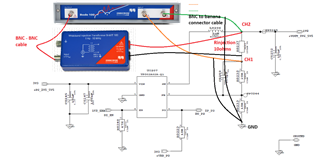
Tool/software:
Hello Team,
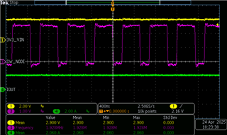
I am using TPS62A02A IC for 1V1, 1V8 and 1V25 (adjustable output voltage from 0.6V to Vin(Vin = 3.3V)). I am trying to measure the stability at maximum load of 2A.
For 1V25, at 25degC, -40degC, 85degC, max load = 2A: the buck output is working fine.
But for 1V1 and 1V8, At 25degC, -40degC and 85degC, max load = 2A, the buck output is turning off. (maximum current withstand-able is 1.4A only)
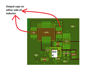
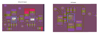
Below is the layout comparison between 1V25 and 1V1-1V8 blocks:
Schematic:
1V8
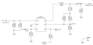
1V1

1V25

Layout:
In datasheet this sentence is given. If this is true, why i got output voltage for 1V25 IC and not for 1V8 and 1V1? Could you please share the results for EVM measurement?

Also in EVM user guide, it shows there should be enough space on the output and input, which wasnt followed in our design, could this be an issue?

Please guide.