This thread has been locked.

If you have a related question, please click the "Ask a related question" button in the top right corner. The newly created question will be automatically linked to this question.

UCC28180: PCB layout review based on UCC28180

Part Number: UCC28180

Tool/software:

Hi dear,

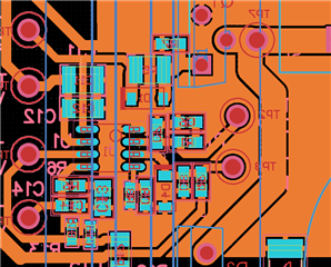
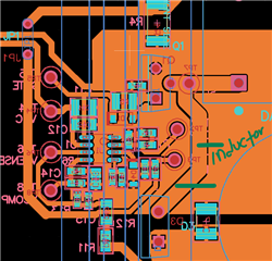
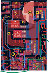
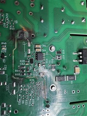
I am design a PFC boost converter based on the example TI has given. However, Upon powering up the PFC boost converter, it blow up. Attached is the schematic, PCB layout (exclude the blue zone, they are not part of the testing- no components are connected), and the blown up traces. 

The nominal spacing is 2.5-3mm. However, the spacing between the ground plane and the PFC controller components is 0.25mm.Kindly review the schematic and check if i have missed out something that May have damaged the board.

The 12V, GND of the PFC controller is supplied with PSU. 

The feedback trace to pin 6 and the 12V to VCC seems to have been damaged once the circuit was energised . 

Boost Converter UCC28180 sch.pdf
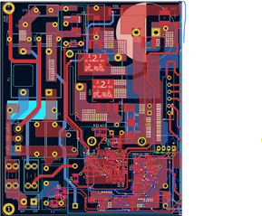
Kind regards,

Bright

  • Hello Bright, 

    I see no significant issue with the schematic diagram. 
    I believe the problem is caused by the PCB layout. 

    The main clue is that: "The feedback trace to pin 6 and the 12V to VCC seems to have been damaged once the circuit was energized."  

    On the board you can see that R30 is the top resistor of the VSENSE divider string and R30 has the high-voltage "DC BUS" net on it. 
    The 12V VCC track is next to the VSENSE divider string and there is a corner of the track where the point is close to the top pad of R30. 

    I think that the DC BUS voltage at R30 arced over to the corner of the VCC track and the arc-current burned out the track and R34 and damaged other components, too. 

    You may have 2.5-3mm spacing in certain parts of your design, but the spacing at the VCC track is not wide enough to prevent the possibility of arcing.
    I suspect that this not the only place where there is insufficient spacing between high-voltage and low-voltage nets.  
    But this is the place where the arc happened.  Maybe there was a sharp point on the solder of the top pad that increased the electric field strength. 

    Whatever the case, I recommend to review the pcb layout and increase spacings between high-voltage and low-voltage nets where necessary. 

    Regards,
    Ulrich

  • Hi Ulrich, 

    Thank you for the swift feedback. 

    How about:

    1. The spacing between the ground plane of the PFC controller and its traces (such as connecting to Pin 1- 7), it is currently 0.25mm, is it enough? or does it have to be 2.5-3mm? See the EVM layout those traces are spacing are thin. Also, is the EVM board coated with conformal or normal solder mask?

    2. The feedback trace runs through the ground plane in my layout and the spacing is 0.25mm, is that sufficient? 

    Kind regards,

    Bright

  • Hello Bright, 

    The issue of proper PCB spacings is outside of the purview of this E2E forum.  We provide support on how to use our controllers in their applications.

    I recommend to find out which particular safety standard applies to your product and study their requirements.
    For example, for many years Information Technology equipment was governed by IEC 60950, but that standard has been replaced by IEC 62368 in recent years.  The standard for your product may be different, but this serves as an example of where to find safety-related and operational spacing requirements. 

    Regards,
    Ulrich  

  • Hi Ulrich,

    Thank you for your feedback. 

    I'm following up on the spacing between ground plane and the controller traces as shown in the UCC28180- EVM board. Whether it is acceptable to have  0.25mm spacing through the ground plane as shown in your EVM. 

    Kind regards

    Bright

  • Hi Bright, 

    In general, low voltage signals can have much smaller spacings between them and their respective GND net (which includes a plane, if any). 

    0.25mm = ~10mil spacing, which is acceptable for the controller voltages on our EVM. 

    Regards,
    Ulrich

  • Hi Ulrich,

    Thank you for the swift reply. 

    Does this imply that the 0.25mm spacing between the ground plane and the low voltage signal of the controller on my layout is okay. Also, the 0.25mm spacing of the feedback trace between ground plane is okay?

    See the attached image below. The part green colour is inductor trace which carries at 350V DC, how come there is small spacing between the inductor and ground pane?

    Kind regards,

    Bright

  • Hi Bright, 

    I am not qualified to provide statements as to whether the spacings on your board conform to the requirements that apply to your product. 
    That is an internal matter within your company. 

    As for the inductor trace question, there are different spacing rules for distance through insulating material versus spacing for distance across insulating material.  Please consult the appropriate safety standard for your product(s) for details.  

    I will not answer further questions on spacing.  
    If you have questions on the use of the UCC28180 or some other TI controller IC, please start a new thread. 

    Regards,
    Ulrich

  • Hi Ulrich,

    Thank you for your swift feedback

  • HI Ulrich,

    I have printed a new Circuit board .


    I wanted ask about the diode required at the ISENSE to ensure that the pins does not go more negative. The ISENSE maximum current is -+1mA. 

    1. Does it mean that  the Resistor in series 221 ohm and a diode with low forward such as MMSD4448 will damage the pin? This is because 1.1V/221 is more than +- 1mA. In this sense. Also the VF of the diode/221 ohms is still more than 1mA. How does it work really?  

    Kind regards,

    Bright

  • The gate signal is coming ON and OFF, I suspect the diode. I was using CDBMT2100-HF but I considering changing to it MMSD4448 

    Kind regards,

    Bright

  • Hi Bright, 

    Normally, the diode on ISENSE input is only effective during the time of inrush current when the PFC controller does not have any control over the peak current charging up the output capacitor to the peak of the input line. 

    During PFC boost switching time, the peak currents will be limited by the current-sense SOC and PCL voltage thresholds at the ISENSE input. 

    Therefore, I don't think that your choice of clamp diode has anything to do with " the gate signal coming ON and OFF". 
    Please provide some waveforms of this symptom, along with information about the test conditions applied to the board when you capture the symptom. 

    Regards,

    Ulrich

  • Hi Ulrich,

    Thank you for the reply. 

    I have removed the Diode at ISENSE. 

    Input Voltage 240 AC (UK Mains)

    After diode bridge rectifier it reads 348V DC

    FeedBack network. R_upper (332k, 332k, 340k) 1%, R_lower 13.7k 1%

    Vout is showing 373-374V (Multimeter)

    I have attached a video (Gate signal) of the waveform. I used a differential probe x50. Is it possible to use single-ended Probe for the Vgs?

    I have attached a video (PSU consumption) showing the power consumption of the VCC, which is intermittent. 

    The VSENSE voltage reading is unstable - see the attached video (Feedback), measurement with a multimeter.

    I can send you the Gerber file of the PCB layout on secured platform if required. However, I have attached part screenshot

    Kind regards,

    Bright

  • Hi Bright, 

    It appears that the video viewing plugin for xxxx.MOV files is not supported by E2E.   (I wasn't aware of this.)

    Can you please try converting them to .mpeg?

    It is possible to use a single-ended probe for Vgs provided that your AC source is isolated from Earth GND
    The oscilloscope is connected to Earth-GND, so wherever the single-ended probe connects its GND wire, that point/net is grounded.
    No other single-ended probes can be GNDed to any other net, because it will short the two nets together through the 'scope.  

    I'll be leaving work for the day soon, so any further replies from me will be tomorrow. 

    Regards,
    Ulrich 

  • Hi Ulrich,

    Thank you for the swift reply. 

    I have re-uploaded  the videos with mpeg. See dropbox link https://www.dropbox.com/scl/fo/hkppsnse9547dug0aar70/ANodZJ6Ogogvy8hyMmTwINw?rlkey=3cva1q9rjr4z9teo3d91q84us&dl=0   . Kindly confirm if you can access it. 

    The AC source is only Line and Neutral (No - EARTH connected) and the Oscilloscope has not EARTH connected. Does it mean that I can use singled-ended Probe at VGS? 

    No other single-ended probes can be GNDed to any other net, because it will short the two nets together through the 'scope.

    Does that mean that I can only use 1 single ended probe and not 2 probes?

    Kind regards,

    Bright

  • Bright,

    As much as we'd like to help you, I think the communication should go through our local FAE channel so it can be more efficient and effective. Please contact our local FAE and we can be connected via them too.

    Thanks for the understanding.