Other Parts Discussed in Thread: BQSTUDIO, BQ25620EVM, EV2400, BQ25620
Tool/software:
Dear Sir,
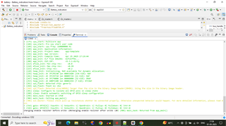
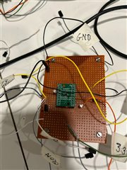
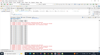
We are testing battery charging circuit using BQ25622RYKR so we are facing some issues. We attached our schematic for your reference.
Issues:
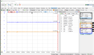
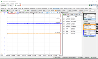
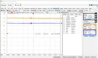
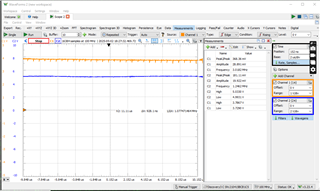
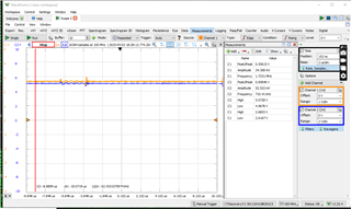
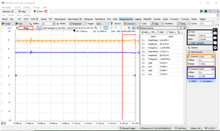
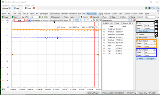
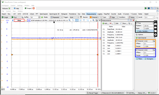
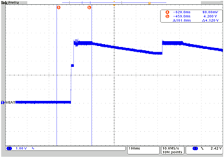
1) When we give input voltage at VBUS so it could not generate VSYS and VBAT.
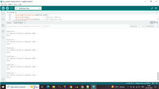
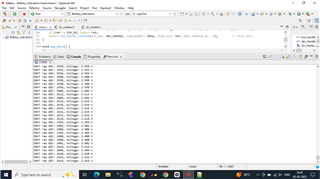
2) In our schematic when we connect VBAT to VSYS load it will work and I2C is Detect but it gives garbage value in12bit ADC.
3) When we give input voltage at VBUS and also connect the battery in VBAT and load VSYS in this case we cant get any output voltage and IC is Heated Extremely.
So please give the solution for our problem so after that we finalize the design and we are planning to use this design in our product in large scale.so give us best guide for the same.AE175_DT_01.01.pdf