This thread has been locked.

If you have a related question, please click the "Ask a related question" button in the top right corner. The newly created question will be automatically linked to this question.

LM5122: The boost converter oscillates when driving a DC motor

Part Number: LM5122
Other Parts Discussed in Thread: LM5121

Tool/software:

Hi,

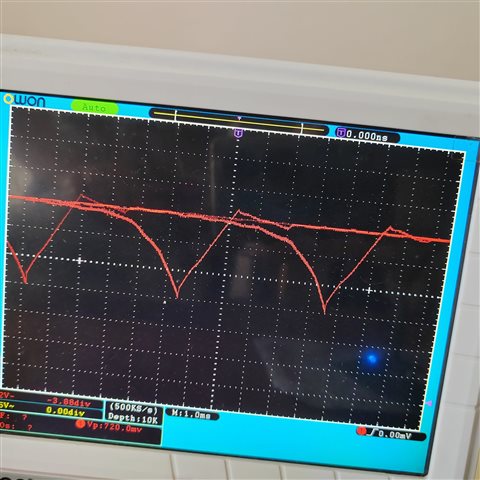
The output of my LM5122-based boost converter is stable at approximately 38 V when the only load is a power LED. However, as soon as I connect a DC motor, the output voltage ramps up and then collapses every 3–5 seconds, repeating this cycle indefinitely.

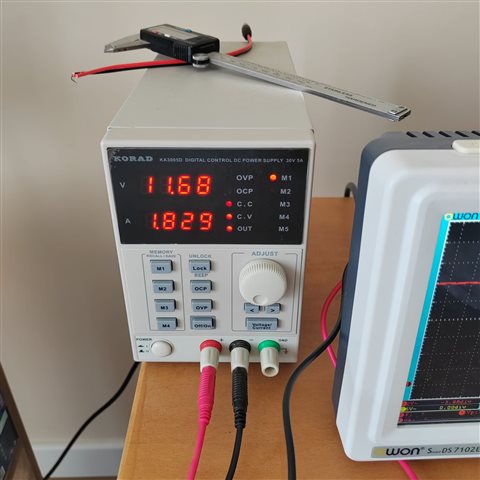
The bench power supply feeding the converter can deliver up to 10 A, which exceeds the motor’s inrush and running current.

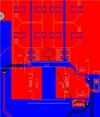
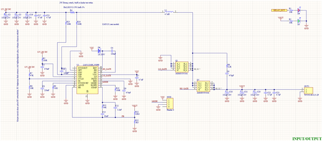
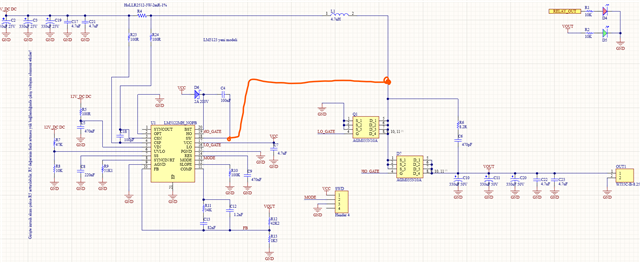
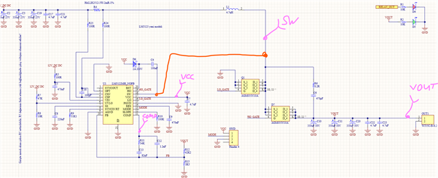
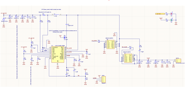
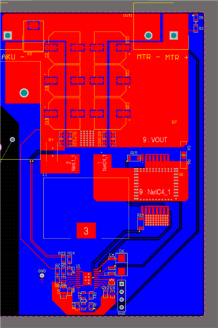
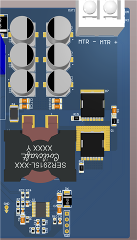
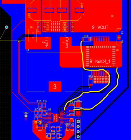
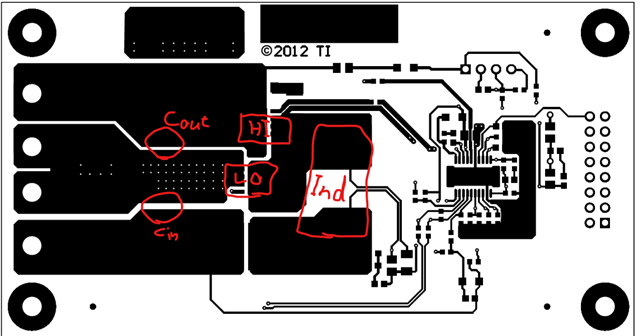
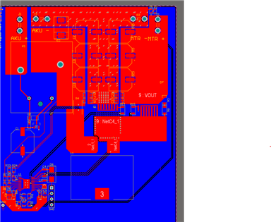
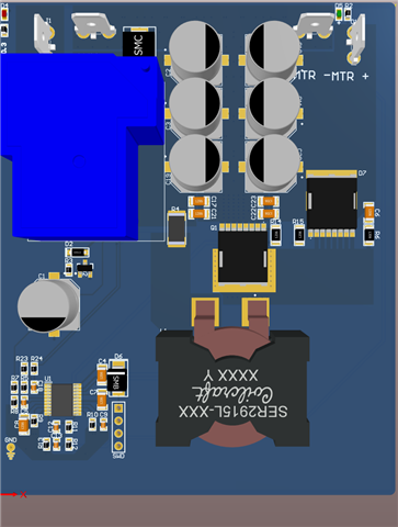
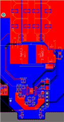
The schematic and PCB layout (attached) were copied from TI’s evaluation board, and I followed the layout guidelines as closely as possible.

What might be causing this periodic rise-and-fall behaviour under motor load, and how can I stabilise the output? Any suggestions for measurements or component changes would be appreciated.

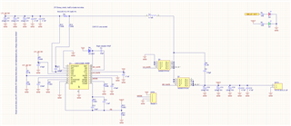
Schmatic Image: https://ibb.co/ycnYxnRS

  • Hi Sinan,

    Thanks for using the e2e forum.
    The pictures you attached seem to be not loading, so I cannot open them.
    Also the link you attached leads to a website which is blocked by our system.

    Could you try to re-attach the waveforms and the schematic?
    To review the design, could you also include the parameters for VIN (min & max), VOUT and max load?

    Thanks and best regards,
    Niklas

  • Hi Niklas,

    I have edited my post and reuploaded the images.

    VIN(min): 10V
    VIN(max): 14V
    VOUT: 37V to 38V

    The load current typically remains around 7–8 A during normal operation. However, it is higher at startup because of the initial mechanical load from the attached gears.

  • Hi Sinan,

    Thanks for the re-upload and the parameters.

    Right now I cannot say what is the root cause for the hiccup oscillation. For this, it would be helpful I you could make waveform measurements during the failure case and measure VOUT and the SW voltage.
    This might show us if it is related to instability of the system.

    I do have some general comments on the design:
    Schematic:
    - C4 is the boostrap capacitor. Is it 10uF or 100nF? 100nF would be a better selection, as this capacitor should be smaller than the VCC cap C7.
    - The compensation should be stable, but you may try another set of values to see if the behavior improves.
    For the given specs, I would recommend to replace R11 & C13 with 34kOhm and 70nF. (Based on our power stage designer calculator tool)

    Layout:
    - Are there any vias placed on the power ground plane near the Cin/Cout caps?
    The loop back from the low side MOSFET GND to the input/output GND is crucial for the power stage and should be kept as short as possible.

    Thanks and best regards,
    Niklas

  • Hi Niklas,

    I’m out of town and will have access to the measurement equipment in about two weeks. I’ll share the measurement results you requested as soon as I return. Thank you.

  • Hi Sinan,

    Thank you for the update.
    I will look forward to your results.

    Best regards,
    Niklas

  • The power supply output is stable at 2A, but after a few seconds it drops to 1A and then returns to 2A again. The power supply is rated for 10A output. I get the same results when testing with a 120A battery. I have uploaded some videos.

  • Hello Sinan Atilla,

    A motor is an inductive load which can cause issues with the regulation of our device. Please check your design with the quickstart calculator: LM5122-BOOST-CALC Calculation tool | TI.com

    Is it possible that the speed of your motor is somehow related to the crossover frequency of the LM5122?

    You could check with adding a big capacitor to the output (make sure the LM5122 is still stable).

    Best regards,
    Brigitte

  • Hello Brigitte,

    I used the calculation tool you shared and made several adjustments, but I’m still getting the same result. I’ve added output capacitors up to 10,000 µF and tried different motors with similar current ratings, yet the issue persists. Interestingly, when I test with a power LED, which draws less current than the motor, the problem does not occur.

    Could you advise on what changes I should make to the output current-limit settings, or recommend a step-up converter better suited for this motor?

  • Hi Sinan,

    Thanks for the feedback.
    Before I recommend further adjustments, can you share the schematic once more with the changes you already performed included?
    I also asked a question on the layout regarding vias on the GND plane. Do you have the answer to this question?

    Layout:
    - Are there any vias placed on the power ground plane near the Cin/Cout caps?
    The loop back from the low side MOSFET GND to the input/output GND is crucial for the power stage and should be kept as short as possible.

    Thanks and best regards,
    Niklas

  • Hi Niklas,

    I’ve just gotten access to the board and manually implemented your GND connection suggestion by drilling a hole in the PCB. With this change, the periodic speed fluctuation every few seconds disappeared, and it now runs stably at the same output voltage. However, under load the output voltage drops to 16 V, while without load, I’m seeing 37 V.

    I suspect the power supply. I’ll try with another one.

  • Hi Sinan,

    I checked the schematic once more and there is one major error I have missed so far.
    Can you please check if there is a connection between the SW pin and the switch node itself?
    Without this, the high side FET cannot turn on properly and you are operating the device as an asynchronous boost just with the body diode of the high side FET.
    This works fine at no load, but at higher load, the high side FET will break eventually.

    Maybe you can add a wire from the solder pad of C4 to the source of the high side MOSFET?

    I am very sorry I missed this in my first review.

    Best regards,
    Niklas

  • Hi Niklas,

    Despite reviewing the EVK schematic and TI tool’s recommended schematics multiple times, I’d missed this critical connection. As you suggested, I bridged C4 to the MOSFET high side with a wire, but it didn’t change the result. The output voltage is around 15.5 V while the input is 12 V. Is there any specific node you’d like me to probe with the oscilloscope? To reiterate, everything appears to be fine at ~2–3 A loads.

  • Hi Sinan,

    Thanks for the update.
    Could you probe the following signals with an oscilloscope:
    - VOUT
    - SW
    - COMP
    - VCC

    Based on this, we should be able to narrow down why VOUT target is not reached.

    Thanks and best regards,
    Niklas

  • Hi Niklas,

    I have uploaded the scope video.

  • Hi Sinan,

    Thanks for recording the waveform behavior.

    It looks to me like the device is switching and tries to boost up the voltage, but then stops for a longer period before resetting.
    This could be related to the hiccup overload protection feature of the device.
    A description is given in the datasheet:

    If the inrush during during start-up is too high, the device will reset and the device never achieve the output voltage target.

    To verify if it really is the hiccup protection, you can replace the C9 capacitor with a 0 Ohm resistor. This will shorten the RES pin to GND and disable the hiccup feature.

    Another option is using a larger sofstart capacitor (C8). This will slow down the voltage ramp up and therefore decreases the overall inrush current.

    Best regards,
    Niklas

  • Hi Niklas,

    As you suggested, I shorted the C9 capacitor to GND (I didn’t have a 0Ω resistor available, so I directly shorted it). For C8, I mounted a 1 µF capacitor. I’m sharing the oscilloscope waveform below.

    At the moment, the circuit no longer goes into a start-stop behavior, however with a 12 V input the output still rises up to a maximum of 15.5 V. My adjustable power supply is set to 12 V / 5.5 A. When I power up the system, the current is around 1.68 A, but the input voltage drops to 11.68 V.

    I’m considering redrawing the circuit and assembling all components on a new PCB to ensure there are no layout or soldering-related issues.


        L1 inductor_inpower supply

    Best regards,


  • Hi Sinan,

    Thanks for the update.
    Even if you disable the hiccup feature, there is still the regular cycle-by-cycle overcurrent protection, so the duty cycle gets limited if the inductor current is too high.
    Checking the layout for any GND shorts is a good idea.
    What are the load conditions if you see 1.8A on the supply? Does this value make sense based on the output load, or are you operation without load on the output?

    Best regards,
    Niklas

  • Hi Niklas,

    I identified the issue as the motor’s startup current not being supported by the power supply or the 24Ah battery. After connecting the battery and the power supply in parallel, I can now achieve 37V at the output under load.

    However, the inductor and MOSFETs have started heating up. I will try to handle this without using a heatsink.
    I am currently using the AGM035N10A MOSFET and the FSA1360-4R7MT inductor.

    The MOSFET is rated at 100V, 112A, 3mΩ@10V, and 104W. I estimate the average input current to be around 27A, with a duty cycle of 0.68. The conduction loss is about 1.3W per MOSFET, and the switching loss is around 4.4W for the high-side MOSFET.

    The inductor has 9mΩ DCR, which results in approximately 6.6W of loss at 27A. Including core loss, I estimate around 8W.

    In total, this adds up to about 20W of loss. I plan to redesign the circuit with a lower DCR inductor and MOSFETs with lower Qg and Rds(on).

    I would also like to add a soft-start of about 1–2 seconds. Do you have any recommendations for implementing this?

    Currently, the system is switching at 250kHz according to the EVM values. Do you see any issue if I reduce the switching frequency to 100kHz? I am considering this to reduce switching losses.

  • Hi Sinan,

    The changes you plan sound reasonable to me.
    You can increase the softstart time by increasing the SS capacitance (C8)
    Reducing the switching frequency to 100kHz is also possible.
    Please use our quickstart calculation tool to see how the recommended values change and select components for compensation, sense resistance and inductor accordingly.
    https://www.ti.com/tool/download/LM5122-BOOST-CALC

    Best regards,
    Niklas

  • Hi Niklas,

    I found that the LM5121 seems more suitable than the LM5122 for motor drive applications. However, when I tried to update my design with the LM5121 using TI Power Designer, it indicated that the LM5121 is not suitable for a 10A, 37V output design. Do you think the LM5121 would be a better choice, or should I stay with the LM5122?

    Best regards,


  • Hi Sinan,

    The main difference between LM5122 and LM5121 is that
    LM5122 has multi phase capability,
    LM5121 has a disconnect FET to reduce inrush currents during turn-on of the power supply or to fully disconnect VOUT from VIN during shutdown state.

    Aside from this, the two devices are similar in regard of functionality and power capability.

    Best regards,
    Niklas

  • Hi Niklas,

    I’m continuing on this topic thread. If it’s not suitable, I can open another one. I plan to continue here until the issues are fully resolved :)

    I’m sharing the schematic and PCB view below, could you take a look?


  • Hi Sinan,

    Thanks for the update and new files.

    I compared the schematic to the previous design and I approve all the changes that have been implemented in the revision.
    The schematic looks good to me now.

    Regarding the layout, there are still some optimizations possible:

    - The SW trace and the HO trace should be routed very close to each other. The SW trace is the return path of the high side driver current, so placing HO and SW close to each other will reduce system noise.
    I highlighted the two traces in yellow.

    - The switch node plane has a lot of vias placed. Are these vias for thermal heat dissipation, or is there another purpose?
    As the SW plane is jumping up and down, it will increase noise the larger the area of the node, especially if it is traversing multiple layers.

    - There are now vias placed to connect the LO MOSFET ground with the input/output ground, which is good.
    The placement of the LO MOSFET itself is still not ideal, as the ground path is rather long. If the MOSFET could be placed above the inductor, the placement would be more ideal. However, I do not know if this is possible due to size constraints.
    EVM reference board:

    Best regards,
    Niklas

  • Hi Niklas,

    Thank you for your support.

    To cool the Q1 MOSFET, I am creating a plane on the bottom layer with the same area as the Q1 pad and using vias to transfer the heat. I would prefer not to add an external heatsink. If you have any other suggestions to improve the cooling with fewer EMI issues, please share them with me.

    I have already made adjustments according to your recommendations. I cannot change the PCB dimensions, and the tall components must remain at the center.

    If you have any further suggestions for this final version, please let me know so I can add them before sending the PCB for prototyping.

    Best regards

  • Hi Sinan,

    Thanks for providing the design changes.
    The new component placement looks very good to me.
    Now, there are very short power stage loops and the trace of SW and HO are also very close to each other.
    Using vias on the SW plane for heat dissipation is okay. Managing thermal behavior and EMI often comes with a trade-off, so it is important to find a balance where both are fulfilled to an acceptable level.

    There are no further change suggestions from my side.

    Best regards,
    Niklas