This thread has been locked.

If you have a related question, please click the "Ask a related question" button in the top right corner. The newly created question will be automatically linked to this question.

LM25011: Designing with LM25011MY

Part Number: LM25011

Tool/software:

Hello Team,
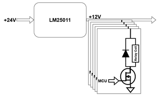
We are using the IC LM25011MY in one of our PCBs.

The input voltage is +24V and the designed output is 12V.

The load is some relays and the maximum load current is just below 1A.

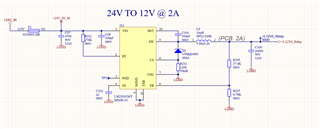
The part number of the inductor is SP52-100K and that of diode is 15MQ040N.

The saturation current of the inductor is close to the load current

All relays are controlled by an MCU.

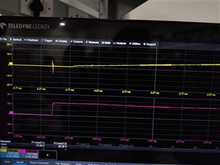
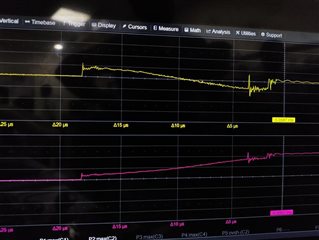
This DC DC got damaged when the MCU is reset.
Now the output is shorted to GND (checked across the diode).

The input is not shorted to GND.

Also, no short between input and output.

We see no reason to damage the DC DC when MCU is reset.

Can you please review the schematic?. And please let us know if there are any other reasons to damage teh IC.

  • Hi,

    Can you probe output voltage waveform when the MCU reset happens? It would also be helpful to see the inductor current waveform.

    Also please try replacing the current sense resistor R111 with a value close to 100 mOhm. With 50 mOhm the current limit set is higher than the saturation current of the inductor which is not recommended.

    Regards,

    Niranjan

  • Hello Niranjan,
    Thank you for the reply.

    As I have mentioned before, the device is damaged and we cannot take the waveform you asked.
    Powering another board without identifying and solving the issue may damage the device.

    When the MCU is reset and start to boot again, the worst case scenario will be all relays will turn on at the same time.
    But still the the total current will be (20 relays * 40mA) 800mA only.

    ..  Now the output is shorted to GND (checked across the diode).
    .. The input is not shorted to GND.
    .. Also, no short between input and output.

    1). Is there any overload protection in the device?
    2). Will this device damage when the +12V output is accidentally touches the ground
    3). What could be the reason for the damage?.

    when the Rsense is set to 100mOhm, what will be the load current?.

    Looking for your reply

  • Hi,

    1) There is an overcurrent protection in the device, the current limit being set by the Rsense value. 

    2) Ideally, no. The OCP should kick in and limit the current through the device.

    My guess is that during the reset a momentary short is happening at the output causing the current to rise rapidly. Usually, this shouldn't be an issue but, with the Rsense value you are currently using (50m) the current limit is around 2.5A. This is higher than the inductor saturation current and might be causing the inductor current to runaway. 

    The recommended practice is to use an inductor with a saturation current higher than the peak current at current limit. With 50m Rsense the peak current limit will be ~ 115m/50m + Ipp = 2.9 A. Since the inductor saturation current is 2.3A this is not recommended. Hence why I asked to try with 100m which will give a peak current of 115m/100m + Ipp = 1.75 A, leaving a good margin from the typical saturation current of the inductor.

    Rsense will not have any effect on the load, just that it will limit the maximum possible load current. With 100m the limit would be ~1.5A which should be sufficient right?

    Regards,

    Niranjan

  • Hello Niranjan,
    Thank you for the reply.

    Sure, we can change the inductor to a high current rated one or we can change the Rsense to 100m.

    Can you please clarify the following doubts I have?.

    1). Can you please review the schematic and please let us know if there are any issues.

    As per the webench, the recommended capacitance at the pin Vin is 1uF and the capacitor at SS was 10nF.
    In our design, it is 100nF and 22nF respectively. Will this create any problem?.
    2). Assume in the worst case the load current is 2A and the inductor current is 2.9A, which is more than the saturation current of the inductor, will this damage the device. In our case the inductor is not damaged.
    3). The +12V out of the DC DC is connected to 26 relay coils.
    Chances are there when MCU is reset the relays can de-energize. We have free wheeling diode across all relay coils. Will this inductive kickback from the relay coil damage the device (since only the output is shorted to GND)?.

    Looking for your reply

  • Hi,

    1) I do not see any issues other than the sense resistor value. At VIN in addition to 100 nF you have a 4700 nF (C97) which is sufficient. Capacitor at SS is just to set the soft-start time so that too should not pose any issue.

    2) Once the inductor saturation current is crossed the current limit may not work properly and the actual peak current can go much higher than the set 2.9A. Since the device is rated for 2A (DC), much higher currents can cause the device to damage even if inductor itself doesn't.

    3) Can you share the part of the schematic showing how the relay coils and diodes are connected to the device?

    Regards,

    Niranjan

  • Hello Niranjan,
    Thank you for your reply.

    The maximum load current is 1A, so the maximum switching current will be less than 2A. Please correct me if I am wrong.

    All the relays (26) are connected to the +12V out of the DC DC.

    Relay MPN - AZSR250-2AE-12D

  • Hi,

    In normal conditions the maximum switching current will be less than 2A. But, in case a temporary short happens at the output, the current limit may not work properly as it is set higher than the saturation current of the inductor. 

    It is difficult to say what is exactly happening when MCU is reset without seeing the waveforms, but I am suspecting that something is causing the current to rapidly rise. If the current limit does not work properly it can exceed the allowable current through the device and damage it. My recommendation is still to change Rsense to 100 mOhm.

    Regards,

    Niranjan

  • Hello Niranjan,
    Thank you for your reply.

    In the attached image below, yellow is the +12V output of the DC DC and the pink color is the +24V input of the DC DC Converter.


    The Yellow output voltage is measured with respect to GND and is going up to -8V when the power is applied to the system.

    when the input voltage is 4V, the output is almost close to 10V and then goes upto -8V. Then increases to designed +12V as expected.


    Also, in our case, all the relays are off initially and only one LED is connected to the +12V output.
    so the total load current will be 0.45mA for LED + the current through the feedback resistor.
    Is there any minimum current requirement for the DC DC converter, in our use case, the load is less than mA.

    Looking for your reply.

  • Hi,

    Can you clarify what the difference in test condition among the two images are? The first image is how the startup is expected to be. 

    In the second image, I see two issues. When input is 4V, output should not be 10V as VOUT cannot be higher than VIN in buck operation. Second is the dip to -8V, does any external change happen when this dip occurs?

    A minimum load of 1 mA is recommended for this device, so it would be better to reduce feedback resistor values to ensure this.

    Regards,

    Niranjan

  • Hello Niranjan,
    Thank you for your reply.
    Sorry for the confusion.

    The second image is a zoomed version of the first waveform.

    Is there any specific reason the output voltage is going to -8V when powered. After this the device works normally.

    we disconnected and connected the 24V input to the DC DC and that is how we measured the waveform.

    , does any external change happen when this dip occurs?

    No, when connected the supply again, this device stopped working

  • Hi,

    From the first image it looks like the input is somehow coupling to the output and causing a ringing. Is there some external path through which this can happen? The device itself should not be able to push VOUT higher than VIN.

    Also, can you clarify the following?

    After this the device works normally

    No, when connected the supply again, this device stopped working

    So the device behaves normally after the dip. But after disconnecting and connecting the power supply it does not work anymore. Is my understanding correct?

    Regards,

    Niranjan

  • Hello Niranjan,

    Thank you for your reply.

    There is nothing in our system connecting the input to the output not even some other DC DC converters.

    But after disconnecting and connecting the power supply it does not work anymore. Is my understanding correct?

    Regards,

    Correct.

    As you can see from the first image, the output was 0v when no input is connected. So we cannot assume that this was the residual voltage from the previous on off cycle as the load current is minimum and there is no other path to discharge the bus 

  • Hi,

    Give me some time to think on this and get back to you. Were the graphs taken with 50 mOhm Rsense or was it increased to 100 mOhm?

    Regards,

    Niranjan

  • Hello Niranjan, 

    This graph is taken when Rsense is 50mOhms.

  • Hi,

    Is the device being hot-plugged? Looking at the VIN waveform, the slew rate appears to be very high. The maximum slew rate recommended for this device is 1 V/us, hence it is not meant to be hot-plugged. This could be the reason the device stops working.

    The high slew rate could also be causing VIN to couple to VOUT though some parasitics. There could also be a component of coupling happening through the probe parasitics. You can try using tip and barrel method to capture VOUT to minimise this.

    In any case, the device is not meant to handle slew rates greater than 1V/us. I would suggest turning the supply on/off rather than hot-plugging to see the startup waveform.

    Regards,

    Niranjan

  • Hello Niranjan,
    Thank you for your reply.

    We are unable to find anything related to the slew rate from the datasheet.
    Can you please show where is it?.

    Also, what will happen we are turning on and off the power supply and still the slew rate of the power supply is above 1v/uS.

    Can we add some extra decoupling capacitors at the input to solve this issue?.

    Looking for your reply.

  • Hi,

    That is a not a specification as such, more of a general recommendation for our buck converters. If the slew rate is too high, it will charge the gate through Cgd of the high side FET, potentially causing damage. If such high slew rates are expected in your application, I would suggest adding some extra capacitors at the input to slow it down.

    As we are discussing further on email, I will close the thread here.

    Regards,

    Niranjan