


Tool/software:
Dear TI Engineer,
We encountered a new issue when using BQ25792, which is that some devices cannot enter charging mode normally after the battery is discharged. We set the charger voltage to 16.8V for 4s battery, and the battery voltage is about 11.4V when the battery is fully discharged.
We have read the values of all registers that can and cannot be charged normally, and the comparison data obtained is as follows:
Abnormal charging register data
Regaddr: 00 01 02 03 04 05 06 07 08 09 0A 0B 0C 0D 0E 0F 10 11 12 13 14 15 16 17 18 19 1A 1B 1C 1D 1E 1F 20 21 22 23 24 25 26 27 28 29 2A 2B 2C 2D 2E 2F 30 31 32 33 34 35 36 37 38 39 3A 3B 3C 3D 3E 3F 40 41 42 43 44 45 46 47 48
data:	 26 06 90 00 64 8B 00 9A C3 05 EA 00 DC 4B 3D A2 85 78 00 61 36 AA C0 7A 55 00 9A 0B 0A 01 C0 00 20 40 00 80 10 00 20 40 00 00 00 00 00 00 B0 00 00 00 31 00 00 3B 04 3B 14 00 00 2C BC 33 14 02 BC 00 4E 00 1E 00 1C 00 08
data:	 26 06 90 00 64 8B 00 9A C3 05 EA 00 DC 4B 3D A2 85 78 00 61 36 AA C0 7A 55 00 9A 0B 0A 01 D0 00 00 00 00 80 10 00 20 40 00 00 00 00 00 00 B0 00 00 00 41 00 00 3A E6 3B 88 00 00 2C 42 40 88 02 D8 00 5A 00 1D 00 1D 00 08
data:	 26 06 90 00 64 8B 00 9A C3 05 EA 00 DC 4B 3D A2 85 78 00 61 36 AA C0 7A 55 00 9A 0B 0A 01 D0 00 00 00 00 80 10 00 20 40 00 00 00 00 00 00 B0 00 00 00 2D 00 00 3B 76 3A 62 00 08 2A EE 44 62 02 1C 00 56 00 00 00 1E 00 08
data:	 26 06 90 00 64 8B 00 9A C3 05 EA 00 DC 4B 3D A2 85 78 00 61 36 AA C0 7A 55 00 9A 0B 0A 01 C0 00 20 40 00 80 10 00 20 40 00 00 00 00 00 00 B0 00 00 00 2D 00 00 3B AA 3A F0 00 14 29 D4 44 F0 02 64 00 4B 00 00 00 03 00 08
data:	 26 06 90 00 64 8B 00 9A C3 05 EA 00 DC 4B 3D A2 85 78 00 61 36 AA C0 7A 55 00 9A 0B 0A 01 D0 00 00 00 00 80 10 00 20 40 00 00 00 00 00 00 B0 00 00 00 2D 00 00 3A E8 3A 9E 00 16 29 DA 44 9E 01 B8 00 4F 00 1D 00 00 00 08
data:	 26 06 90 00 64 8B 00 9A C3 05 EA 00 DC 4B 3D A2 85 78 00 61 36 AA C0 7A 55 00 9A 0B 0A 01 C0 00 20 40 00 80 10 00 20 40 00 00 00 00 00 00 B0 00 00 00 2D 00 00 3B 04 3A 18 00 00 29 DA 45 18 01 96 00 4B 00 1D 00 00 00 08
data:	 26 06 90 00 64 8B 00 9A C3 05 EA 00 DC 4B 3D A2 85 78 00 61 36 AA C0 7A 55 00 9A 0B 0A 01 D0 00

Normal charging register data :
Regaddr: 00 01 02 03 04 05 06 07 08 09 0A 0B 0C 0D 0E 0F 10 11 12 13 14 15 16 17 18 19 1A 1B 1C 1D 1E 1F 20 21 22 23 24 25 26 27 28 29 2A 2B 2C 2D 2E 2F 30 31 32 33 34 35 36 37 38 39 3A 3B 3C 3D 3E 3F 40 41 42 43 44 45 46 47 48
data:	 26 06 90 00 64 8B 00 9A C3 05 EA 00 DC 4B 3D A2 85 78 00 61 36 AA C0 7A 55 00 9A 0B 4A 01 D0 00 00 00 00 00 00 00 00 00 00 00 00 00 00 00 B0 00 00 00 AD 00 42 3A FA 3A EE 00 12 2D 82 2F EE 02 EE 00 4F 00 1B 00 2F 00 08
data:	 26 06 90 00 64 8B 00 9A C3 05 EA 00 DC 4B 3D A2 85 78 00 61 36 AA C0 7A 55 00 9A 0B 4A 01 D0 00 00 00 00 00 00 00 00 00 00 00 00 00 00 00 B0 00 00 00 AC 00 42 3B 16 3A EE 00 06 2D 82 2F EE 02 EE 00 4E 00 1B 00 2D 00 08
data:	 26 06 90 00 64 8B 00 9A C3 05 EA 00 DC 4B 3D A2 85 78 00 61 36 AA C0 7A 55 00 9A 0B 4A 01 D0 00 00 00 00 00 00 00 00 00 00 00 00 00 00 00 B0 00 00 00 AC 00 44 3B 18 3A EE 00 14 2D 82 2F EE 02 EE 00 4F 00 1A 00 2C 00 08
data:	 26 06 90 00 64 8B 00 9A C3 05 EA 00 DC 4B 3D A2 85 78 00 61 36 AA C0 7A 55 00 9A 0B 4A 01 D0 00 00 00 00 00 00 00 00 00 00 00 00 00 00 00 B0 00 00 00 AF 00 3E 3B 18 3A EE 00 14 2D 82 2F EE 02 EE 00 4F 00 19 00 2F 00 08

Compare the differences in register data:
Regaddr:                 1E  20  21  23  24  26  27  3132  3334
Abnormal charging data: C0  20  40  80  10  20  40  0031  0000
Normal charging data:   D0  00  00  00  00  00  00  00AD  0042


Functional definition of differentiation:
1Eh[bit4]:
VSYS Regulation Status (forward mode)
Type : R
POR: 0b
0h = Not in VSYSMIN regulation (VBAT > VSYSMIN)
1h = In VSYSMIN regulation (VBAT < VSYSMIN)


20h[bit5]:
VBAT over-voltage status
Type : R
POR: 0b
0h = Normal
1h = Device in over voltage protection

21h[bit6]:
VSYS over-voltage status
Type : R
POR: 0b
0h = Normal
1h = Device in SYS over-voltage protection

23h[bit7]
Charge status flag
Type : R
POR: 0b
0h = Normal
1h = Charge status changed

24h[bit4]
VSYSMIN regulation flag
Type : R
POR: 0b
0h = Normal
1h = Entered or existed VSYSMIN regulation

26h[bit5]
VBAT over-voltage flag
Type : R
POR: 0b
0h = Normal
1h = Enter VBAT OVP

27h[bit6]
VSYS over-voltage flag
Type : R
POR: 0b
0h = Normal
1h = Stop switching due to system over-voltage
From the register recording, there are some protection happens when the battery cannot charing. Do you have any ideas about this question?
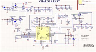
The schematic is as below:
The link to another post on my case is
Thanks,
Best Regards
