This thread has been locked.

If you have a related question, please click the "Ask a related question" button in the top right corner. The newly created question will be automatically linked to this question.

LMZ13608: LMZ13608TZ short on pin 9 ?

Part Number: LMZ13608

Tool/software:

Dear TI,

I have some question on LMZ13608TZ.

Me and my team used this DCDC in many occasion with the same scheme and on the same board without problem but recently it seems unstable.
We use it to create a 5V output, that power up a CM4, from a 24 V input. Randomly (sometimes after a few hour, sometimes after days) the Vout goes up, over the 5V, and we see the pin 9 burned.

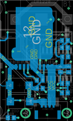
The PCB is the same as the old one that worked without problem, it's a different lot but it seems that the problem it's not in the different production.

Do you have any idea I can work with to resolve the issue? 

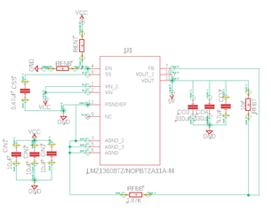
Here the schematic we are using:

Thank you for your disponibility,
Chiara

  • Hi Chiara,

    Please send over the layout as well, so we can review this as well. 

    Additionally, on previous working boards was the schematic the same?

    Thank you,

    Joshua Austria

  • Hi Joshua,

    Yes the schematic is the same, as it is the layout. They must do the same thing, is just a new round of pcb and LMZ13608.

    Hope this may help.

    Thank you!
    Chiara

  • Hi Chiara, 

    I have a couple of notes to make about the schematic and layout.

    Schematic:

    • What is the rating of your output and input capacitors? TI recommends that capacitors are rated for at least 2x the voltages they are set to experience to avoid significant de-rating and to ensure the proper amount of output capacitance is being provided on the necessary pins.
    • Is there an input filter network on VIN? The layout looks to have a couple of extra components on VCC that don't seem to be present on the schematic. If so, please provide this.
    • Have you tested the stability of this configuration? By interrupting the feedback path with a small resistance (around 10-50ohms) you can inject a small signal to test the schematic's loop response. If you have this please share it, and if you do not, are you able to take a stability measurement?

    Layout:

    • I am unsure of how components to ground are connected. Is there a ground plane or a hidden topside ground plane that is not shown in the screenshot? Please share all relevant layers and planes if this is true.
    • The VIN to GND loop is relatively large on this layout, and this will increase the amount of noise that is generated by the system as a whole. As this trace is fairly close to feedback, I am worried about the potential for noise to couple on feedback and interrupt the regulation of the system.
    • There are very few thermal vias and the GND plane is relatively small. TI recommends a thermal via and ground pour similar to the layout below for adequate heat sinking. Over extended use, this can cause the device to fail if the junction temperature rises above the recommended operating temperature for this device (125C). 
    • Do you have access to an EVM? If not, my recommendation would be to order one and conduct an ABA swap between your board and the EVM. This will allow us to test the two solutions over time and help determine if it is a part issue or an application issue.

    Thank you,

    Joshua Austria

  • Hi Joshua,

    thank you for your detailed response. I'll try to do the same by following your list.

    Schematic:

    • The CO3 and CO4 are tantalum capacitors of 330uF (0,33mF) 6,3V 2917. (They're actually not x2 of the output voltage)
      The CO2 is a 47uF 6,3V X5R 0805 capacitor
      CSS is a 0,47uF (470nF) 50V X7R 0805 capacitor
      CIN 1,2 and 3 are 10uF 35V X5R 0805 capacitors
      Can mildly high temperature have an impact on the rated voltage?
    • No, there's no additional filter. I suppose you are referring to the two resistors up on the right side of the image. They are not soldered and I think (the first schematic is not mine) they were used in case they needed to enlarge the FB resistors.
    • I didn't think to this test, thank you. I'll try as soon as I can.


    Layout:

    • Yes, there is a GND plane. Actually, all 4 layers of the schematic have GND plane and are connected together through vias spreaded along all the board.
    • To reduce the loop, in the future, do you recommend using a polygon for Vcc and keep it on the right side? As to separate more the Input with the ground and the output? I'm working on improving my knoledge on ground loop so every help is appreciated.
    • That's definitely something we need to do. For now we try to keep the temperature under 80C. We put the pcb on a dissipating support as to avoid temperature problem.
    • No, I don't have an EVM but I'll try to get one. For now we have done test on the boards we have by using an electric load. With the same PCB but different LMZ13608 we see different results. Sometimes the 9 pin seems to short-circuit and the CO3 nearly explode after 2 hours. With others LMZ13608 (same components, PCB, PCB supports and ambient) the test run for days without problem and without raising the temperature. So I'm not sure what test I should work on the EVM as it's not a repeatable event.
      [to make it more clear: with same PCB I mean that they are from the same lot. But I also made a try with the same board by soldering two different LMZ13608 acquired at the same time. One time it lasted, one time it burned]

    I'll for sure work on you suggestions.

    Thank you very much,
    Chiara

  • Hi Chiara,

    I see. Thanks for confirming all those items. 

    I am not sure why pin 9 would burn in any case as that is a NC pin for this device. In the case where the device failed, is the board hot? What does pin 9 short circuit to? 

    I am also not sure how the device temperature would not rise with the non-shorted units. I would still expect the device to generate heat as it turns on. Can you please detail your process and the tests you are running on these boards?

    In the future for reducing the loop, I would look to the layout screenshot provided previously. This is also in the application section of the datasheet. This gives plenty of insight into what the optimal layout looks like for this part and the reasoning behind it. 

    Are you ensuring that you are abiding by the reflow parameters when reworking/mounting these devices? If the reflow guidelines are exceeded, the device may be damaged internally. You can find the reflow parameters for this part in the datasheet.

    As for the EVM test, I would conduct the same tests that you are doing on your boards on the EVM, to see if the modules on the EVM experience similar behavior/failure. While it is not necessarily repeatable, I would like to rule out as many variables as possible. This way, we can determine with better certainty if the issue is a layout or device issue. Please let me know how bode testing and EVM testing goes with the part. I look forward to your feedback.

    Thank you,

    Joshua Austria

  • Hi,

    As I have not heard from you in some time, I will close this thread for now. Please feel free to reopen the thread should you have anything additional to comment.

    Thank you,

    Joshua Austria

  • Yes, thank you!

    I'm sorry it took me so long. 
    It seems the problem was indeed the temperature, the capacitors where stressed too much and the short had repercussion on the DC/DC.

    Sorry again for being late and thanks again for the detailed help.

  • Hi Chiara,

    No problem. I am glad your issue was resolved!

    Thank you,

    Joshua Austria