Other Parts Discussed in Thread: BQ25792
Tool/software:
Hi,
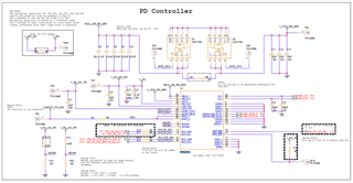
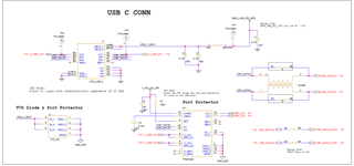
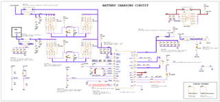
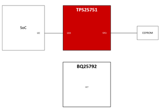
We are using the TPS25751 in our design to implement USB Power Delivery input for a 4-cell (4S) battery charger, based on the BQ25792 IC.
The charger handles a battery voltage range of 12V to 16.8V with a Load current ranging from 3.9A to 2.7A.
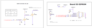
I have attached the schematics for your review. Kindly take a moment to check and share your valuable feedback or suggestions.
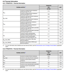
Additionally, we would appreciate it if you could share the power dissipation data for the TPS25751 under these operating conditions, as it is required for our thermal analysis.