Part Number: LM5117
Tool/software:
In my CC/CV DC-DC converter project I need to put 2 MOSFET in parallel to manage more current and I need a very high peak current to charge quickly the two gates, so I choose le LM5117 because it has 2.2Amps Gate peak current.
Reading the datasheet I learned the VCC regulator can supply maximum 30mA (typ 5.8mA) of current towards the VCC pin.
On the VCC pin there is 7.6Volts with 30mA of maximum current available to supply the HO Driver and LO driver.
The question is: How the Drivers can deliver 2.2Amps or 3.3Amps to the MOSFETs gates if their power supply can deliver only 30mA?
Do they maybe get peak energy from Cvcc capacitor?

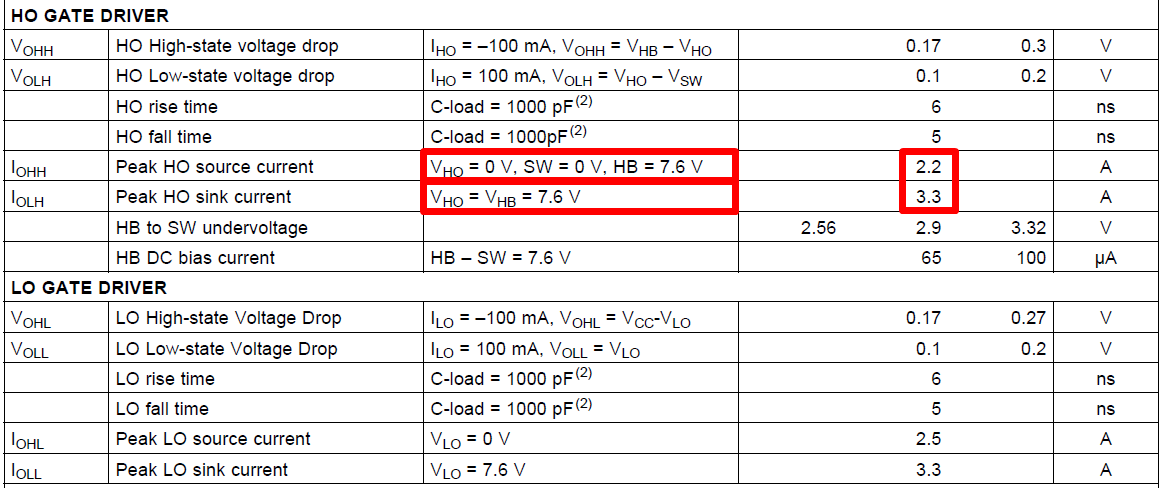
In the above table the peak source current, for the HO driver, is 2.2Amps with the conditions "Vho=0V" and "Vsw=0V", but this condition will depolarize the QH N-MOS (Vgs=0) and the driver current will be in "sink" mode... sorry but I don't understand.
The same for the "sink" condition: sink should be when the current flows from the gate capacitance to the driver port... but this is impossible with "Vho=Vhb=7.6Volts".
Can you explain me what is the logic?
Can you confirm me the peak current in the MOSFETs gate is about 2.2Amps during the gate charging?
thank you,
Michele Faini