This thread has been locked.

If you have a related question, please click the "Ask a related question" button in the top right corner. The newly created question will be automatically linked to this question.

TPS25751EVM: Control charger IC via PD controller

Part Number: TPS25751EVM
Other Parts Discussed in Thread: BQ25798, TPS25751

Tool/software:

Hi Team:

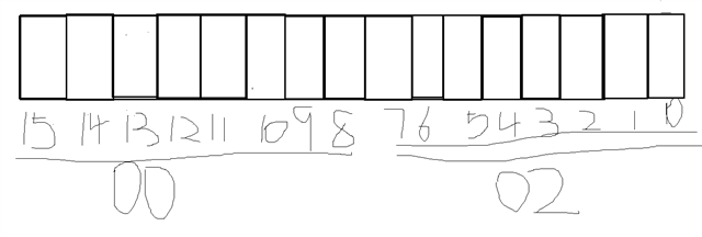
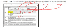
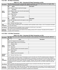
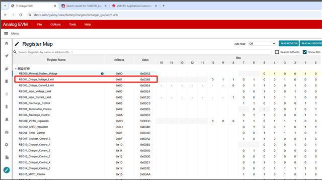
I encountered a problem while using TPS25751 to read and write registers of BQ25798 using IIC. If I directly read the data from the register(0x01), the value is 00.But the result read by EE colleague on the computer is 0x0348, If I first write the data into the register and then read it,(Write 0x0346 to the 0x01 register), The data read back is also 0x3C46.But the data read by EE colleagues on the computer is still 0x0348.
Could you please help me check what could be causing it, such as code errors or hardware issues
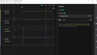
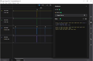
Here is my reading and writing function and the returned log

[MSDK][TPS25751] read_reg: reg 08, value 04
[MSDK][TPS25751] CMD1 Status: 04 00 00 00 00

[MSDK][TPS25751] Read Data from BQ25798: 40 03  01 02 00 00  00 00

#define TPS25751_REG_CMD1   0x08
#define TPS25751_REG_DATA1  0x09
static int tps25751_read_bq25798_iindpm(const msdk_device_t *dev, uint8_t *data_out)
{
    int ret = MSDK_STATUS__ERROR;

    // Step 1: Write DATA1 (0x09), with data to set up TPS25751 to read from BQ25798
  
    uint8_t setup_data[4];
    setup_data[0] = 0x03;       // length = 3 bytes
    setup_data[1] = 0x6B;       // BQ25798 I2C slave address
    setup_data[2] = 0x01;       // target register in BQ25798
    setup_data[3] = 0x02;       // read 2 bytes
    ret = write_reg(dev, TPS25751_REG_DATA1, setup_data, sizeof(setup_data));
    if (ret != MSDK_STATUS__OK) {
        MSDK_LOG_ERR("Failed to write TPS25751 DATA1");
        return ret;
    }

    // Step 2: Write CMD1 (0x08) with 'I2Cr' command
    uint8_t i2cr_cmd[5] = { 0x04, 'I', '2', 'C', 'r' };
    ret = write_reg(dev, TPS25751_REG_CMD1 , i2cr_cmd, sizeof(i2cr_cmd));
    if (ret != MSDK_STATUS__OK) {
        MSDK_LOG_ERR("Failed to write TPS25751 CMD1 for I2Cr");
        return ret;
    }

    // Step 3: Read CMD1 back to confirm command executed (should return 0x00 0x00 0x00 0x00)
    uint8_t cmd_status[5] = {0};
    ret = read_reg(dev, TPS25751_REG_CMD1, cmd_status, sizeof(cmd_status));
    if (ret != MSDK_STATUS__OK) {
        MSDK_LOG_ERR("Failed to read TPS25751 CMD1 status");
        return ret;
    }
	MSDK_LOG_DBG("CMD1 Status: %02X %02X %02X %02X %02X", 
              cmd_status[0], cmd_status[1], cmd_status[2], cmd_status[3],cmd_status[4]);

    // Step 4: Read back the 2 bytes result from DATA1 (0x09)
    ret = read_reg(dev, TPS25751_REG_DATA1, data_out, 4);
    if (ret != MSDK_STATUS__OK) {
        MSDK_LOG_ERR("Failed to read response from TPS25750 DATA1");
        return ret;
    }
	MSDK_LOG_DBG("Read Data from BQ25798: %02X %02X %02X %02X", data_out[0], data_out[1],data_out[2],data_out[3]);
    return MSDK_STATUS__OK;
}


static int tps25751_write_bq25798_iindpm(const msdk_device_t *dev)
{
    int ret = MSDK_STATUS__ERROR;

    // Step 1: Write to TPS25751's DATA1 register (0x09)
    // Data: 05 6b 03 06 00 C8
    // -> Length = 5
    // -> Slave address = 0x6B
    // -> Write operation (0x03)
    // -> Register = 0x01
    // -> Data = 0x0346
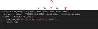
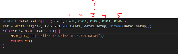
    uint8_t data1_setup[] = { 0x05, 0x6B, 0x03, 0x06, 0x03, 0x46 };
    ret = write_reg(dev, TPS25751_REG_DATA1, data1_setup, sizeof(data1_setup));
    if (ret != MSDK_STATUS__OK) {
        MSDK_LOG_ERR("Failed to write TPS25751 DATA1");
        return ret;
    }

    // Optional: Verify write to DATA1
    uint8_t data1_readback[6] = {0};
    ret = read_reg(dev, TPS25751_REG_DATA1, data1_readback, sizeof(data1_readback));
    if (ret != MSDK_STATUS__OK) {
        MSDK_LOG_ERR("Failed to read back TPS25750 DATA1");
        return ret;
    }
    MSDK_LOG_DBG("DATA1 Readback: %02X %02X %02X %02X %02X %02X",
        data1_readback[0], data1_readback[1], data1_readback[2],
        data1_readback[3], data1_readback[4], data1_readback[5]);

    // Step 2: Write 'I2Cw' to CMD1 register (0x08)
    uint8_t i2cw_cmd[] = { 0x04, 'I', '2', 'C', 'w' };  
    ret = write_reg(dev, TPS25751_REG_CMD1, i2cw_cmd, sizeof(i2cw_cmd));
    if (ret != MSDK_STATUS__OK) {
        MSDK_LOG_ERR("Failed to send I2Cw command to CMD1");
        return ret;
    }

    // Step 3: Read back CMD1 status
    uint8_t cmd_status[5] = {0};
    ret = read_reg(dev, TPS25751_CMD1_REG, cmd_status, sizeof(cmd_status));
    if (ret != MSDK_STATUS__OK) {
        MSDK_LOG_ERR("Failed to read CMD1 status\n");
        return ret;
    }

    MSDK_LOG_DBG("CMD1 Status: %02X %02X %02X %02X %02X",
        cmd_status[0], cmd_status[1], cmd_status[2], cmd_status[3],cmd_status[4]);


    return MSDK_STATUS__OK;
}


Best Regards!
Iris

  • Hi Iris,

    Please share the json used with the TPS25751 to generate the binary.

    Please provide a digital scope log of the I2C transactions to the BQ device in each of the cases so we can confirm what is actually being written to the BQ Device.

    1. I2C when I2Cw and I2Cr is used through the TPS25751
    2. I2C read when the PC reads from the BQ directly

    The PD controller will configure some of the BQ registers if a BQ device is selected in the GUI configuration. Is the BQ being read in similar situations? Both systems have a TPS25751 with the same Binary flashed, power bring-up and connections are the same?

    Are there any differences in the setup between you and your colleague?

    Thanks and Regards,

    Chris

  • Hi Chris:

    Sorry, I didn't use the JSON you mentioned to use with the TPS25751 to generate the binary

    1.The log for I2C when I2Cw and I2Cr are used through the TPS25751 is as follows:Read Data from BQ25798: 40 03  06 02 00 C8  00 00(Write 0x00C8 to register 06 first, and then read the obtained log)

    2.The log for I2C read when the PC reads from the BQ directly is as follows:[MSDK][TPS25751] Read Data from BQ25798: 40 03  01 02 00 00  00 00(Directly read the 0x01 register of BQ25798)


    The relevant read-write functions were provided yesterday

    There is no difference in settings compared to colleagues

    Best Regards!

    Iris

  • Hi Iris,

    How did you generate the binary? How are you loading a patch bundle to the TPS25751 on boot up, are you using an EEPROM or an I2C MCU? The loading of the patch bundle is an important step in the boot process. The bundle can affect the operation of the I2C lines on the PD controller.

    Can you confirm that the I2Cw and I2Cr are working properly? I.e. when you send the commands, if you connect a digital analyzer or oscope to the I2Cc lines, does the I2C look correct?

    Please capture the I2Cc lines when you send these commands and share the captures.

    Why are you writing to reserved bits in the I2Cw pahyload, is this a typo?

    Thanks and Regards,

    Chris

  • Hi Chris:

    Is the binary file you are referring to the one used for PTCH Mode to APP Mode? If so, we generated it using the upper computer tool provided by TI. However, we have not yet implemented this Step of PTCH Mode to APP Mode and it is stuck in the tenth step. The printed log does not recognize our patch and we are currently seeking technical support.


    May I ask if the implementation of this PD reading BQ25798 through IIC must be based on a successful loading patch, that is, if the PD is in APP mode?

    I have the EEPROM disconnected on the EVM (removing JP16)

    Should the written array be uint8_t data1_setup []={0x05, 0x6B, 0x00, 0x02, 0x03, 0x46}?


    0x05 refers to the size of this I2C write packet ;

    0x6B refers to BQ25798 device address ;

    0x00 refers  to reserved bit(The top eight bits in bytes2-3);

    0x02 refers to Number of bytes in the transaction payload;

    0x03 0x46 refer to represents the data written to the register;

    Best Regards!
    Iris

  • Hi Iris,

    This is for the input Data for the I2Cw command, correct?

    Per the TRM, it should look like [0x05, 0x6B, 0x02, 0x00, "BQ REGISTER OFFSET", 0x03, 0x46]

    You need to follow the format defined in the TRM.

    Thanks and Regards,

    Chris

  • Hi Chris,
    Shouldn't the identifiers 0-15 in bytes2-3 be as shown in the figure? 8-15 corresponds to the upper eight bits, which is byte2, i.e. 0x00, while 0-7 corresponds to the lower eight bits, which is byte3, i.e. 0x02. Is my understanding incorrect?

    Best Regards!

    Iris

  • Hi Iris,

    Yes, that is why your original formatting is incorrect, you ignored the reserved bits and were writing to them.

    Thanks and Regards,

    Chris

  • Also Yes, the PD controller should be in APP mode for the I2Cr and I2Cw 4CC commands to be used.

    Thanks and Regards,

    Chris

  • Hi Chris,

    ok, Thank you very much for pointing out the error message. 

    I have made the modifications as per your instructions, and the code is as follows. Even after successfully loading PATCH, I was able to read the relevant information of the charger, but the returned result is still incorrect. The code and related logs are as follows. Could you please help me check what problem is causing it? Thank you very much!((I first write data to the register before reading it))
    Also, I would like to ask if your PD needs to perform any initialization work on the charger when reading its related information through IIC?
    Or have you used a logic analyzer tool to capture the relevant timing diagram of PD reading the charger through IIC? Can you share it with us? We can compare based on the timing chart!

    But using my unmodified code before, in the case of successful PATC LOAD, it is possible to read and write the value of the 0x01 register normally, but there are exceptions. Some registers fail to read the default value but write successfully, while others succeed in reading the default value but fail to read again after writing
    Thank you so much!


    #define TPS25751_REG_CMD1   0x08
    #define TPS25751_REG_DATA1  0x09
    static int tps25751_read_bq25798_iindpm(const msdk_device_t *dev, uint8_t *data_out)
    {
        int ret = MSDK_STATUS__ERROR;
     
        // Step 1: Write DATA1 (0x09), with data to set up TPS25751 to read from BQ25798
        uint8_t setup_data[4];
        setup_data[0] = 0x03;       // length = 3 bytes
        setup_data[1] = 0x6B;       // BQ25798 I2C slave address
        setup_data[2] = 0x06;       // target register in BQ25798
        setup_data[3] = 0x02;       // read 2 bytes
        ret = write_reg(dev, TPS25751_REG_DATA1, setup_data, sizeof(setup_data));
        if (ret != MSDK_STATUS__OK) {
            MSDK_LOG_ERR("Failed to write TPS25751 DATA1");
            return ret;
        }
        else {
            MSDK_LOG_DBG("TPS25751 DATA1 written successfully");
        }
     
        // Step 2: Write CMD1 (0x08) with 'I2Cr' command
        uint8_t i2cr_cmd[5] = { 0x04, 'I', '2', 'C', 'r' };
        ret = write_reg(dev, TPS25751_REG_CMD1 , i2cr_cmd, sizeof(i2cr_cmd));
        if (ret != MSDK_STATUS__OK) {
            MSDK_LOG_ERR("Failed to write TPS25751 CMD1 for I2Cr");
            return ret;
        }
        else {
            MSDK_LOG_DBG("TPS25751 CMD1 for I2Cr written successfully");
        }
     
        // Step 3: Read CMD1 back to confirm command executed (should return 0x00 0x00 0x00 0x00)
        uint8_t cmd_status[5] = {0};
        ret = read_reg(dev, TPS25751_REG_CMD1, cmd_status, sizeof(cmd_status));
        if (ret != MSDK_STATUS__OK) {
            MSDK_LOG_ERR("Failed to read TPS25751 CMD1 status");
            return ret;
        }
        else {
            MSDK_LOG_DBG("TPS25751 CMD1 status read successfully");
            MSDK_LOG_DBG("CMD1 Status: %02X %02X %02X %02X %02X",
                    cmd_status[0], cmd_status[1], cmd_status[2], cmd_status[3],cmd_status[4]);
        }
        /*if (cmd_status[1] != 0x00 || cmd_status[2] != 0x00 || cmd_status[3] != 0x00 || cmd_status[4] != 0x00) {
            MSDK_LOG_ERR("TPS25751 I2Cr command failed to execute properly");
            return MSDK_STATUS__ERROR;
        }*/
    	msdk_time_delay_ms(50);
        // Step 4: Read back the 8 bytes result from DATA1 (0x09)
        ret = read_reg(dev, TPS25751_REG_DATA1, data_out, 8);
        if (ret != MSDK_STATUS__OK) {
            MSDK_LOG_ERR("Failed to read response from TPS25750 DATA1");
            return ret;
        }
        MSDK_LOG_DBG("Read Data from BQ25798: %02X %02X %02X %02X %02X %02X %02X %02X", data_out[0], data_out[1],data_out[2], data_out[3],data_out[4], data_out[5],data_out[6], data_out[7]);
        return MSDK_STATUS__OK;
    }


    static int tps25751_write_bq25798_iindpm(const msdk_device_t *dev)
    {
        int ret = MSDK_STATUS__ERROR;
    	uint8_t data1_setup[] = { 0x06, 0x6B, 0x02, 0x00, 0x06, 0x00, 0xC8 };
        ret = write_reg(dev, TPS25751_REG_DATA1, data1_setup, sizeof(data1_setup));
        if (ret != MSDK_STATUS__OK) {
            MSDK_LOG_ERR("Failed to write TPS25751 DATA1");
            return ret;
        }
    
        // Optional: Verify write to DATA1
        uint8_t data1_readback[8] = {0};
        ret = read_reg(dev, TPS25751_REG_DATA1, data1_readback, sizeof(data1_readback));
        if (ret != MSDK_STATUS__OK) {
            MSDK_LOG_ERR("Failed to read back TPS25750 DATA1");
            return ret;
        }
        MSDK_LOG_DBG("DATA1 Readback: %02X %02X %02X %02X %02X %02X %02X %02X",
            data1_readback[0], data1_readback[1], data1_readback[2],
            data1_readback[3], data1_readback[4], data1_readback[5], data1_readback[6], data1_readback[7]);
    
        // Step 2: Write 'I2Cw' to CMD1 register (0x08)
        uint8_t i2cw_cmd[] = { 0x04, 'I', '2', 'C', 'w' };  
        ret = write_reg(dev, TPS25751_REG_CMD1, i2cw_cmd, sizeof(i2cw_cmd));
        if (ret != MSDK_STATUS__OK) {
            MSDK_LOG_ERR("Failed to send I2Cw command to CMD1");
            return ret;
        }
    
        // Step 3: Read back CMD1 status
        uint8_t cmd_status[5] = {0};
        ret = read_reg(dev, TPS25751_REG_CMD1, cmd_status, sizeof(cmd_status));
        if (ret != MSDK_STATUS__OK) {
            MSDK_LOG_ERR("Failed to read CMD1 status\n");
            return ret;
        }
    
        MSDK_LOG_DBG("CMD1 Status: %02X %02X %02X %02X %02X",
            cmd_status[0], cmd_status[1], cmd_status[2], cmd_status[3],cmd_status[4]);
    
    
        return MSDK_STATUS__OK;
    }
        179 5.803896       179        MCU  20         [M:msdk C:info F: L: ]: [MSDK][TPS25751] tps25751_init: dev 0x082dfba0
        180 5.803904       179        MCU  16         [M:msdk C:info F: L: ]: [MSDK][TPS25751] tps25751 init
        181 5.803909       179        MCU  16         [M:msdk C:info F: L: ]: [MSDK][TPS25751] i2c initial success.
        182 5.803914       184        MCU  16         [M:msdk C:info F: L: ]: [MSDK][TPS25751] tps25751_init_success
        183 5.803919       185        MCU  20         [M:msdk C:info F: L: ]: [MSDK][TPS25751] tps25751_init: dev 0x082dfbc0
        184 5.803925       185        MCU  16         [M:msdk C:info F: L: ]: [MSDK][TPS25751] tps25751 init
        186 5.803939       185        MCU  16         [M:msdk C:info F: L: ]: [MSDK][TPS25751] i2c initial success.
        187 5.803944       190        MCU  16         [M:msdk C:info F: L: ]: [MSDK][TPS25751] tps25751_init_patch_success
        791 5.881114       280        MCU  24         [M:msdk C:info F: L: ]: [MSDK][TPS25751] read_reg: reg 14, value 0b
        792 5.881118       280        MCU  16         [M:msdk C:info F: L: ]: [MSDK][TPS25751] INT_EVENT1 ReadyForPatch bit is ready for patching.
        794 5.881127       281        MCU  64         [M:msdk C:info F: L: ]: [MSDK][TPS25751] Step 1:  0B 00 00 00 00 00 00 00 00 00 00 02
        796 5.881140       282        MCU  24         [M:msdk C:info F: L: ]: [MSDK][TPS25751] read_reg: reg 03, value 04
        797 5.881144       282        MCU  16         [M:msdk C:info F: L: ]: [MSDK][TPS25751] PD controller is ready for patching.
        798 5.881147       282        MCU  36         [M:msdk C:info F: L: ]: [MSDK][TPS25751] Step 2: 04 50 54 43 48 
        801 5.881163       284        MCU  24         [M:msdk C:info F: L: ]: [MSDK][TPS25751] write_reg: reg 09, value 06
        802 5.881167       284        MCU  44         [M:msdk C:info F: L: ]: [MSDK][TPS25751]  Step 3: 06 80 33 00 00 35 32
        816 5.916705       292        MCU  24         [M:msdk C:info F: L: ]: [MSDK][TPS25751] write_reg: reg 08, value 04
        817 5.916718       292        MCU  36         [M:msdk C:info F: L: ]: [MSDK][TPS25751] Step 4: 04 50 42 4D 73
        867 5.917162       300        MCU  24         [M:msdk C:info F: L: ]: [MSDK][TPS25751] read_reg: reg 08, value 04
        868 5.917171       300        MCU  40         [M:msdk C:info F: L: ]: [MSDK][TPS25751] Step 5: 04 00 00 00 00 00
        883 5.917307       302        MCU  24         [M:msdk C:info F: L: ]: [MSDK][TPS25751] read_reg: reg 09, value 40
        884 5.917315       302        MCU  88         [M:msdk C:info F: L: ]: [MSDK][TPS25751] Step 6: 40 00 00 00 00 00 00 00 00 00 00 00 00 00 00 00 00 00
        885 5.917374       302        MCU  20         [M:msdk C:info F: L: ]: [MSDK][TPS25751] tps25751_write_patch patch size 13184
       1009 7.309955       1686       MCU  24         [M:msdk C:info F: L: ]: [MSDK][TPS25751] write_reg: reg 08, value 04
       1010 7.309980       1686       MCU  40         [M:msdk C:info F: L: ]: [MSDK][TPS25751] Step 8: 04 50 42 4D 63 06
       1011 7.309995       1687       MCU  24         [M:msdk C:info F: L: ]: [MSDK][TPS25751] read_reg: reg 08, value 04
       1012 7.310010       1698       MCU  24         [M:msdk C:info F: L: ]: [MSDK][TPS25751] read_reg: reg 08, value 04
       1013 7.310023       1709       MCU  24         [M:msdk C:info F: L: ]: [MSDK][TPS25751] read_reg: reg 08, value 04
       1014 7.326735       1721       MCU  24         [M:msdk C:info F: L: ]: [MSDK][TPS25751] read_reg: reg 08, value 04
       1015 7.341932       1732       MCU  24         [M:msdk C:info F: L: ]: [MSDK][TPS25751] read_reg: reg 08, value 04
       1016 7.341952       1743       MCU  24         [M:msdk C:info F: L: ]: [MSDK][TPS25751] read_reg: reg 08, value 04
       1017 7.358392       1754       MCU  24         [M:msdk C:info F: L: ]: [MSDK][TPS25751] read_reg: reg 08, value 04
       1018 7.378352       1766       MCU  24         [M:msdk C:info F: L: ]: [MSDK][TPS25751] read_reg: reg 08, value 04
       1019 7.378367       1766       MCU  16         [M:msdk C:info F: L: ]: [MSDK][TPS25751] Confirm CMD1 is cleared.
       1020 7.378372       1766       MCU  40         [M:msdk C:info F: L: ]: [MSDK][TPS25751]  Step 9 :04 00 00 00 00 00
       1021 7.411073       1788       MCU  24         [M:msdk C:info F: L: ]: [MSDK][TPS25751] read_reg: reg 09, value 40
       1022 7.411090       1788       MCU  88         [M:msdk C:info F: L: ]: [MSDK][TPS25751] Step 10: 40 00 00 00 00 00 00 00 00 00 00 00 00 00 00 00 00 00
       1023 7.411105       1788       MCU  88         [M:msdk C:info F: L: ]: [MSDK][TPS25751] Step 10: 00 00 00 00 00 00 00 00 00 00 00 00 00 00 00 00 00 00
       1024 7.411120       1788       MCU  32         [M:msdk C:info F: L: ]: [MSDK][TPS25751] Step 10 :00 00 00 00
       1025 7.411126       1800       MCU  24         [M:msdk C:info F: L: ]: [MSDK][TPS25751] read_reg: reg 14, value 0b
       1026 7.411131       1800       MCU  40         [M:msdk C:info F: L: ]: [MSDK][TPS25751] Step 11: 0B 00 00 00 00 00
       1027 7.440942       1821       MCU  24         [M:msdk C:info F: L: ]: [MSDK][TPS25751] read_reg: reg 03, value 04
       1028 7.440969       1821       MCU  40         [M:msdk C:info F: L: ]: [MSDK][TPS25751] Step 12:04 41 50 50 20 00
       1029 7.440982       1821       MCU  16         [M:msdk C:info F: L: ]: [MSDK][TPS25751] TPS25751 patch bundle loaded successfully, device is in APP mode
       1030 7.441137       1823       MCU  24         [M:msdk C:info F: L: ]: [MSDK][TPS25751] write_reg: reg 09, value 06
       1031 7.441152       1825       MCU  24         [M:msdk C:info F: L: ]: [MSDK][TPS25751] read_reg: reg 09, value 40
       1032 7.441159       1825       MCU  48         [M:msdk C:info F: L: ]: [MSDK][TPS25751] DATA1 Readback: 40 6B 02 00 06 00 C8 05
       1033 7.441171       1826       MCU  24         [M:msdk C:info F: L: ]: [MSDK][TPS25751] write_reg: reg 08, value 04
       1034 7.441177       1829       MCU  24         [M:msdk C:info F: L: ]: [MSDK][TPS25751] read_reg: reg 08, value 04
       1035 7.441183       1829       MCU  36         [M:msdk C:info F: L: ]: [MSDK][TPS25751] CMD1 Status: 04 00 00 00 00
       1046 7.944724       2330       MCU  24         [M:msdk C:info F: L: ]: [MSDK][TPS25751] write_reg: reg 09, value 03
       1047 7.944735       2330       MCU  16         [M:msdk C:info F: L: ]: [MSDK][TPS25751] TPS25751 DATA1 written successfully
       1048 7.944739       2331       MCU  24         [M:msdk C:info F: L: ]: [MSDK][TPS25751] write_reg: reg 08, value 04
       1049 7.944742       2331       MCU  16         [M:msdk C:info F: L: ]: [MSDK][TPS25751] TPS25751 CMD1 for I2Cr written successfully
       1050 7.944745       2333       MCU  24         [M:msdk C:info F: L: ]: [MSDK][TPS25751] read_reg: reg 08, value 04
       1051 7.944748       2333       MCU  16         [M:msdk C:info F: L: ]: [MSDK][TPS25751] TPS25751 CMD1 status read successfully
       1052 7.944751       2333       MCU  36         [M:msdk C:info F: L: ]: [MSDK][TPS25751] CMD1 Status: 04 00 00 00 00
       1053 7.996859       2385       MCU  24         [M:msdk C:info F: L: ]: [MSDK][TPS25751] read_reg: reg 09, value 40
       1054 7.996876       2385       MCU  48         [M:msdk C:info F: L: ]: [MSDK][TPS25751] Read Data from BQ25798: 40 00 00 0A 00 00 00 00
    

    Bset Regards!

    Iris

  • Hi Iris,

    If I understand correctly, the I2Cr and I2Cw commands are partially working? Sometimes it works correctly, others, not so much?

    Can you share a log of the I2Cc to BQ bus during these failures, and explain what I2Cr and I2Cw commands are being sent at specific times? This way we can see what you are writing as commands to the PD controller and we can confirm we see or don't see the activity on the I2Cc lines. I needto see the actualI2C communication on the bus to confirm where the issue is occurring.

    How much time do you wait between I2Cr and I2Cw commands? Per the TRM, we do expect significant time between successive reads and writes.

    Also, I would like to ask if your PD needs to perform any initialization work on the charger when reading its related information through IIC?

    The PD controller will configure a couple BQ25798 registers on bootup if you are using a configuration with the BQ devices selected. You should be able to see the I2Cc bus active on boot if you connect a digital analyzer.

    Thanks and Regards,

    Chris

  • The PD controller will configure a couple BQ25798 registers on bootup if you are using a configuration with the BQ devices selected. You should be able to see the I2Cc bus active on boot if you connect a digital analyzer.

    Hi Chris,

    Can we really read and write the registers configured by PD at startup? What are these registers?

    Best regards!

    Iris

  • Hi Iris,

    Can we really read and write the registers configured by PD at startup? What are these registers?

    The comment I made was that the TPS25751 automatically configures some of the BQ25798 registers on it's own on bootup. If you have a digital analyzer, you should be able to see the I2Cc bus active and will see those I2C writes.

    You cannot change these default writes. You can see what the writes are with a digital analyzer.


    What is the issue you are still seeing?

    If I understand correctly, the I2Cr and I2Cw commands are partially working? Sometimes it works correctly, others, not so much?

    Is this still the main issue?

    Have you looked into adding delays between I2Cw and I2Cr commands?

    Thanks and Regards,

    Chris

  • Hi Iris,

    Apologies for the confusion, it just came to my attention that the way you were originally using the I2Cw command is correct. There is a bug in the TPS25751TRM where that reserved bit is not used. See the correct table below, we are working on updating it.

    See an example log of the I2Cw and Read below. You can use this as reference for your development.

    I2Cw to peripheral at Device address 0x6B. Writing to register 0x81, payload of 0x01

    I2Cr to peripheral at Device address 0x6B. Reading from register 0x81, reading 0x01.

    The I2Cr format is correct. Apologies for the confusion here.

    Thanks and Regards,

    Chris