This thread has been locked.

If you have a related question, please click the "Ask a related question" button in the top right corner. The newly created question will be automatically linked to this question.

TPSM82864A: Noise on VIN

Part Number: TPSM82864A
Other Parts Discussed in Thread: TPS82130, TPSM82866

Tool/software:

Hello,
we are facing noise pickup on a new prototype board featuring several TI step-down switchers.
We must generate several voltages in the 1V0 ... 3V3 range that "gather" underneath an FPGA (core voltage, aux voltage, several I/O bank voltages).

The board features 3 TPSM82864 and 2 TPS82130. All are using the same 5V VIN. The TPSMs are running in forced PWM mode (with external FB divider).
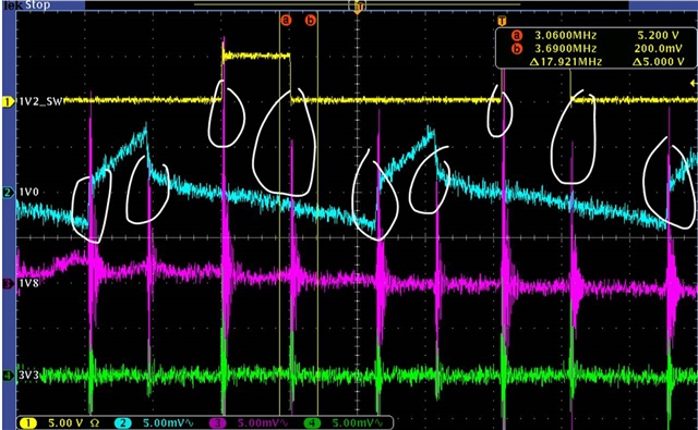
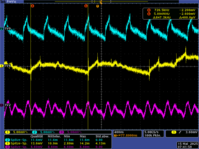
We (seem to) have evaluated that much, that the (internal) switching of the TPSMs is "generating" the noise that is seen on the TPS82130 output voltages. The TPSM output voltages seem to be fine (just normal ripple in the range 10mVpp, no pickup noise here). 

The TPS82130 output voltage (5V VIN, 1.8V VOUT) shows the expected ripple (in frequency and p-p voltage), overlayed by 120mVpp pickup noise "peaks" (noise is rather wide in spectrum, around 500MHz). We have "pinned" the noise peaks to the switching moments of the 3 (free running) TPSMs (scope shot). Looking at the TPSM SW pin, this one is generating really fast switching edges.
The noise is already present at the TPS82130 VIN (5V), so it may be that the noise that has initially been detected at the TPS82130 output (we are having micro-coax connectors on our onboard output voltages that connect via 50R + u-coax/SMA-50R-cable to the BNC connector on the scope 1Meg input) is just passed through by the TPS82130 (and so becomes visible at its output). The noise is not present (or at least not measured that high) in the area were the 5V source enters the board). So it seems the 5V = VIN noise is generated on board at the times the TPSMs are switching.

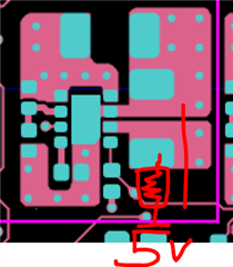
Layer stack is L1 (Top), L2 (GND), L3 (Signal), L4 (Signal), L5 (GND), L6 (Split Power 5V0 = VIN, 1V0, 1V2, 2V5), L7 (Split Power 1V8, 3V3), L8 (GND), L9 (Signal), L10 (Signal), L11 (GND), L12 (Bottom).
TPSMs: CIN 22uF, COUT 2x 22uF. TPS82130: CIN 22uF, COUT 22uF.

Any ideas were to look at? We seem to know who is "initiating" the noise, but what happens exactly? What can be improved in the layout? Should we have added some 1..10nF caps to the TPSM or TPS inputs? Can anything be done at the SW pin (snubber etc.)?

Thanks,

  • In the scope shot above, the 3V3 TPSM has been disabled. The remaining (active) TPSMs are for 1V2 and 1V0. 1V8 is the TPS82130 that picks up the noise. 1V0 shows the corresponding TPSM output, 1V2_SW shows the SW node of the 1V2 TPSM (it had not been that clear from the output waveform when this TPSM really switches). The cursor window shows nothing in particular.

  • Hi,

    Thanks for sharing the waveform.

    How does the ripple/noise look when no other scope channels are connected to anything?  Noise, from SW, can couple between the channels in the scope.

    In many systems, where multiple power converters share the same input voltage, ferrite beads are commonly used on the input of each switcher so that the noise from one of them does not appear on the shared input bus.

    Noise may also be coupling from the input to the output, through the PCB layout.

    Can you share the layout?  We can check for such a coupling path and if there is a suitable place to add a ferrite bead.

    Thanks,

    Chris

  • Hi Chris,

    Noise stays the same with only one scope channel active and connected.

    Yes, we should have added some ferrite beads at the inputs. I think we did not care that much since there is no "analog" function on this one (no ADCs, DACs). However this was rather unexpected (the TPSM is a new part for us) and concern now is for PLLs and overall EMI.

    Yes I could share the layout (with TI). But could you provide a kind of "direct contact" for the layout data? What format? Gerber?

    Thanks,

  • Thanks for confirming.

    You should be able to click on my name or click on the chat bubble on the top right to start a 'conversation' with me.  This is a private message channel.

    I can view most PCB files in their native format (Altium, Cadence, etc.).  What tool are you using?

    Chris

  • ... this is a Zuken (Classic) Cadstar PCB design. Do you have a viewer for this one?

  • No, I'm not familiar with that one.

    Can you send pdfs of each layer and/or screen captures?

    Chris

  • Hi Chris, I have added more information in a privat meassage. Thanks for having a look at it.

  • Thanks for sending.

    Is the other TPS82130 (the one closer/adjacent to the TPSM82866) showing any noise/issues?  The TPSM82866's Vout plane is directly adjacent to the Vin plane to that TPS82130.

    Yes, the common 5Vin plane is adjacent to 2 of the output planes on layer 6.  So, noise could be coupling there.

    Is it possible to run this test?  Cut the Vin plane to the troubled TPS82130, between the cap and the vias.  Then, supply 5V to the cap from an independent lab power supply.  Is the noise still there on the output?

    You could also try powering that cap from the 5V on the board, through a ferrite bead to remove the board's noise from that rail.

    Chris

  • Hi Chris,

    The other TPS82130 (the one between the 1V8 TPS and the 1V0 TPSM) is not fitted/populated.

    As suggested, we have cut the 1V8 TPS82130 VIN pins & CIN pads from the (two) VCC plane vias on that top-sub-plane, and have connected a dedicated 5V DC source directly to CIN.
    We get the following results (the TPS82130 is in PSM mode all the time here):

    Case (1) 1V8 VIN & EN ON (from dedicated 5V source) and main VCC (TPSM 1V0 VIN & 1V2 VIN) OFF
    >>> We see no level or noise on 1V0 VOUT (as expected), we see typical ripple on 1V8 VOUT (appr. 20mVpp) and some switching noise on 1V8 VIN (that does not come from the R&S lab DC source but seems to correspond with the 1V8 TPS82130's own switching).

    Case (2) 1V8 VIN & EN ON (from dedicated 5V source) and main VCC (TPSM 1V0 VIN & 1V2 VIN) ON
    >>> We see typical ripple on 1V0 VOUT, we see the high switching noise on 1V8 VOUT and (as it seems, only) the TPS82130's own switching noise (low freq) on 1V8 VIN. We definitely see switching noise peaks on 1V8 VOUT while the 1V8 VIN shows none (is very quiet).

    Case (3) 1V8 VIN & EN OFF (from dedicated 5V source) and main VCC (TPSM 1V0 VIN & 1V2 VIN) ON >>>
    We see typical ripple on 1V0 VOUT, we see no level or noise on 1V8 VIN, we see the high switching noise on 1V8 VOUT.

    So it seems that the TPSM V_IN/I_IN noise (board VCC 5V) couples to the 1V8 VOUT (not to the 1V8 VIN).

    Not sure if this would be because of a high delta current (on main VCC) or because of a rapid 5V delta voltage on the SW pad.

    Maybe we have a coupling between L6 (relativly narrow Vcc channel) & L7 (1V8) overlap region as shown in the picture? But that would only "explain" a coupling between 1V2_I_IN and 1V8 VOUT, not between 1V0_I_IN (the 1V0 TPSM is located on the right side of the 1V8 TPS82130 and the main VCC enters from the right side of the PCB)?

  • Thanks for running that test.

    Yes, the noise can be coupling from the 5Vin to the 1.8Vout where those planes overlap.  To test that theory, you could cut out the vias on the Vin to the 1V0 TPSM and apply an external 5V to that Vin.  That would remove the TPSM's noise from the internal VIN plane.

    Do all the regulators in the design share a common 5Vin plane, which is on layer 6?  I thought that was the case.  I don't understand your comment: But that would only "explain" a coupling between 1V2_I_IN and 1V8 VOUT, not between 1V0_I_IN

    Chris

  • ... OK, I will try the additional test.

    Correct, all on-board PS have the same +5V Vin that has a plane area on L6. My comment was, because I'm not sure about the root cause. If this is because of voltage (high freq noise) coupling between L7 plane areas overlapping with the 5V VIN plane segment on L6 (e.g. because of plane areas on adjacent "100u gap" planes acting as a capacitor), then please forget my comment. For the comment I was thinking about rapid input current changes on the TPSM Vin inputs with a high current density in the relatively narrow 5V "channel" on L6 (see the marking in the previous picture) that would induce voltages on the L7 plane areas. However, only the 1V2 TPSM is on the left side of the 5V plane "bottleneck" shown in the picture. So I thought that would not explain the 1V0 TPSM impact on the 1V8 noise since that TPSM is on the right (= main source) side of the 5V "bottleneck" on L6 and would not send any current through the "bottleneck".

  • ... just an update: I now have cut the 5V plane vias from the CIN/VIN top sub-planes at the TPSMs and added a ferrit bead (for now, the closest at hand) in-between.  Looks much better now (only the TPS's own and much lower switching noise on the 1V8 now). So most likely, we would add these for the series production.

    Can we improve anything regarding the TPSM VIN/PGND <> CIN connection in the layout? I mean, could we do anything better here so that we would have less VIN switching noise from the TPSMs in the first place (even without ferrit bead)? The current CIN to VIN/PGND implementation looks pretty none-improvable to me. Maybe CIN capacitor choise?

  • Great!  Glad we know what the cause is, at least.

    Yes, you can try using an additional small case size, small value Cin located right next to the device and see how this effects the noise on the other rails.

    I recommend starting with the smallest case size you are allowed to use (0402, 0201, or smaller) as these will have less ESL.  Typical values that have their lowest impedance around 500 MHz are 1000pF and below.  You could use a spectrum analyzer to see what frequency is appearing on the other rail, but I'm guessing that it's in the ~500 MHz area.

    Also, what part number are you using for Cin?  I don't believe I ever checked that.

    Thanks,

    Chris

  • Chris, the part currently used is CL31A226KAHNNN (22uF 10% 25V X5R 1206) (as a single C_in on each TPSM).

  • Thanks.

    It should help to use a smaller case size capacitor, such as 0805 or 0603.  Here are 2 options from Samsung that are in stock on digikey:

    CL21A226MAYNNNE

    CL10A226MP8NUNE

    Chris