This thread has been locked.

If you have a related question, please click the "Ask a related question" button in the top right corner. The newly created question will be automatically linked to this question.

TPS23753A: Non-isolated PoE 24V Output

Part Number: TPS23753A


Tool/software:

Hi,

Based on the previous thread discussing how to modify the design to achieve a 24V output, which can be found at the following link:


e2e.ti.com/.../tps23753a-how-to-design-for-non-isolated-poe-with-an-output-of-24v-0-5a


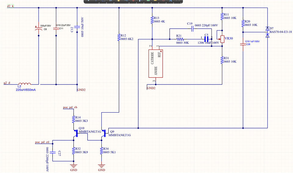
I tried modifying the PMP40355 as per your suggestion to achieve a 24V output by changing the following components:

  • U5 to AS431

  • R30 to 35.7K

  • R31 to 4K

  • R13 to 4K

  • L2 to 330uH

However, I’m a bit confused by your instruction: “Adjust the D2, D2 snubber, output capacitor with higher current rating accordingly.”
Could you please clarify what exactly should be adjusted in those components?

Also, I couldn't find the actual values for the following components. Could you please let me know their specifications?

  • Q1

  • Q9

  • Q10

  • D2

  • D7

I’m aiming for a 24V 0.5A output.
If there is anything else I need to modify in the design to achieve this, I’d appreciate your guidance.

  • Hi Romi,

    Thanks for reaching out! We will look into your question and get back to you in 2-4 business days.

    Best regards,

    Diang

  • Hi, thank you for your reply. Of course, I’m happy to wait for your response.

  • Hi Romi,

    Adjust C13 which are snubber circuit to 100V rating. You can keep same values of R3 and C13 for now and adjust it accordingly during test to have acceptable ripple 

    Q1, Q9, Q10: you can use MMBTA56LT1G and MMBTA06-7-F, or similar BJT with 80V rating. 

    D2: PDS3100Q-13 or similar

    D7: BAS70-04-E3-18 or similar

    Best regards,

    Diang

  • Is the value of D1 appropriate as it is? It appears to be 12V, whereas Q1 — an NPN transistor (MMBTA06-7-F) — has a maximum V<sub>BE</sub> rating of around 5V.
    Should D1 be replaced with, for example, a 3.3V or a Zener diode in the range of 2.5V to 5V, to avoid exceeding the V<sub>BE</sub> limit of the NPN transistor?

    Would replacing the NPN transistor (MMBTA06-7-F) with an N-channel MOSFET provide any significant efficiency benefits?

  • Hi Romi,

    I am currently in timebank and will back on Wednesday. Sorry a delay on the replay and thanks for your patience!

    Best regards,

    Diang 

    Thanks 

  • Hi, I don’t mind waiting until you have time to reply. In the meantime, I also have a few additional questions I’d like to ask.

    I think I made a mistake in calculating the voltage divider for the REF pin of U5. Initially, R30 and R31 were used together with R11, but I have now removed R11 and changed R30 to 34.4kΩ.
    Does this adjustment look correct?

    I would also like to verify the values of surrounding components after replacing U5 with AS431:

    Are the values of R13, R21, C19, and C5 appropriate for the AS431? Or were they selected based on a previous version of U5 and may no longer be suitable?

    Are R12 and R34 appropriate for the current PNP transistor Q9 (MMBTA56LT1G)? Or were they originally selected for a different transistor?

    Similarly for Q10, are R14 and R32 suitable for the new PNP transistor MMBTA56LT1G?

    Is R20 properly sized for the current Schottky diode replacement, BAS70-04-E3-18?

    In addition to the fixed 24V output version, I’ve also built an adjustable version of the design, instead of relying on a fixed resistor ratio, which may be difficult to precisely achieve due to resistor tolerance. In this version, I use a potentiometer (VR30) as shown in the attached schematic.

    I’m using:

    • R11 = 10k

    • R31 = 10k

    • VR30 = 100k

    With this setup, I’m able to adjust the output voltage from 5V to 30V, allowing fine tuning to exactly match the desired output by adjusting the potentiometer.

    Does this approach seem correct and recommended?

    Also, I’d like to ask about the components such as 3314G-1-104E, C8, and others that are connected to the V-OUT negative rail. In the reference design, they don't appear to connect directly to the same GND as components like R32 or R34, so in my schematic I labeled this as GND2.

    Should this GND2 be considered the main ground reference for the entire application circuit (including MCU, LDO, etc.), or is it intended to be a separate ground that must not be tied together with the signal ground or the primary-side GND?

    Any guidance or confirmation would be greatly appreciated. Thank you

  • Hi Romi,

    I am currently in timebank and will back on Wednesday. Sorry a delay on the replay and thanks for your patience!

    Best regards,

    Diang 

  • Hi Romi,

    Please see my comments below: 

    Is the value of D1 appropriate as it is? It appears to be 12V, whereas Q1 — an NPN transistor (MMBTA06-7-F) — has a maximum V<sub>BE</sub> rating of around 5V.

    You should keep D1 = 12V and a NPN. This NPN + 12V Zener is a linear regulator to provide 12V to the VC.

    • R11 = 10k

    • R31 = 10k

    • VR30 = 100k

    If REF = 2.5V, using the formula as: Vout = 2.5V / 10k * (100k+10k+10k) = 30V. When VR is smaller you can get a lower Vout. Yes you can make it adjustable. But L2 value may be not optimized at 30Vout or 5Vout.   

    I think I made a mistake in calculating the voltage divider for the REF pin of U5. Initially, R30 and R31 were used together with R11, but I have now removed R11 and changed R30 to 34.4kΩ.
    Does this adjustment look correct?

    Your phase/gain margin may shifts when you changing R11 values. But you could start with the values you proposed

    Should this GND2 be considered the main ground reference for the entire application circuit (including MCU, LDO, etc.), or is it intended to be a separate ground that must not be tied together with the signal ground or the primary-side GND?

    It depends on the application. But generally GND2 is considered as the main ground for the application load. 

    Besides, you could consider increasing R12 from 6.2k to ~18k for Q10's BREBO rating. 

    Best regards,

    Diang