


Other Parts Discussed in Thread: CSD18543Q3A
Tool/software:
Hi
The inrush current comes out too high when starting up.
Is there any way to improve it?
The schematic cannot be disclosed for security reasons.
Can you tell me how I can deliver it personally?
Input:15V
Output:24V 3.5A
*Waveform
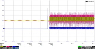
CH1 gate
CH2 Drain Voltage
CH3 Drain Current
Thanks


