This thread has been locked.

If you have a related question, please click the "Ask a related question" button in the top right corner. The newly created question will be automatically linked to this question.

TPS552892: Schematic/Layout Review

Part Number: TPS552892
Other Parts Discussed in Thread: , TPS55289-Q1

Tool/software:

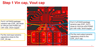
Hello, please review layout and schematic. 

It is meant for supplying a BLDC motor driver board.

Vout = 20V (may change to 15V)

Vin = 10-20V

Iout,max = 2A

Thanks!

(Also, what is difference tween TPS552892 and TPS552892-Q1?)

(I have the feedback path from Rfbt and Rfbb running beneath the IC, is this not advisable?)
(Is it advisable to place a capacitor across Rfbb to smooth out the signal on FB?)

  • Hello, to add to this: I removed any copper beneath the inductor. Also, I added an optional snubber circuit (2.2R w/ 2.2nF cap) on the underside. Thanks.

  • Hi Desmond,

    Thank you for reaching out. TPS55289-Q1 is used for automotive and TPS552892 is used for non-auto.

    About the schematic,

    1.Recommend to add RC snubber in SW1 and SW2. 

    2.There is only one output cap in Vout. Is there more in load side?

    Layout is poor to me. Please follow this layout guideline:7271.TPS55289 Layout Guideline.pdf

    I have the feedback path from Rfbt and Rfbb running beneath the IC, is this not advisable?

    If there is a full GND layer between top layer and signal layer, no issue.

    (Is it advisable to place a capacitor across Rfbb to smooth out the signal on FB?)

    Not advisable. Avoid introduce pole and zero to affect loop stability.

    Regards,

    Mulin

  • Thank you. Here is updated layout:

    I tried to follow the layout guideline as closely as possible, and there is indeed more 22uF capacitors on the load side. There is ground plane on inner layer and bottom layer, and I moved the resistors/capacitors around to mimic the guideline. I also added a 10nF capacitor to DITH/SYNC to ground; is this required? I had it grounded before.

    Also, here is updated schematic, I placed optional snubber circuitry on bottom side:

  • Hi Desmond,

    Due to bandwidth limitation, I will look into this later.

    Regards,

    Mulin

  • Hi Desmond,

     I think the layout improves a lot but still several points to modify.

    1.  GND of Cin and Cout should be connected with GND pin with below.

    2. pin 1, 2, 5, 6 should also be connected to AGND.

    3. thermal vias connection.

    Regards,

    Mulin