This thread has been locked.

If you have a related question, please click the "Ask a related question" button in the top right corner. The newly created question will be automatically linked to this question.

UCC28180: TIDA-00779 Unstable Vout

Part Number: UCC28180
Other Parts Discussed in Thread: TIDA-00779,

Tool/software:

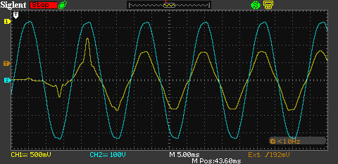
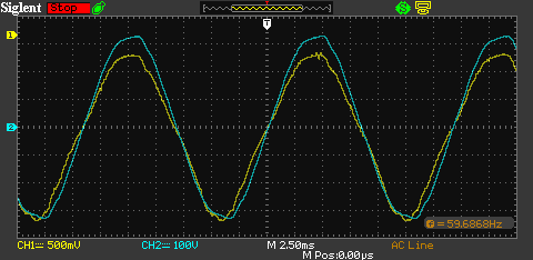
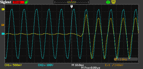
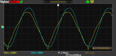
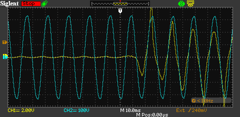
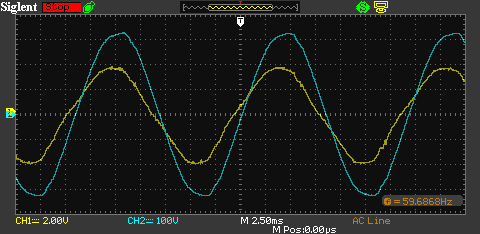
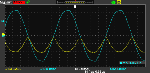
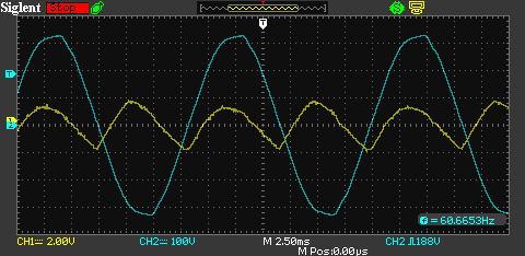
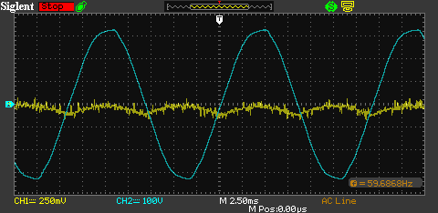
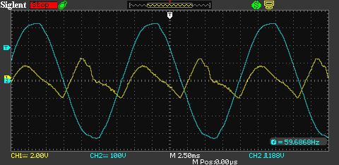
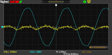
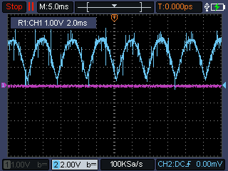
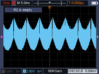
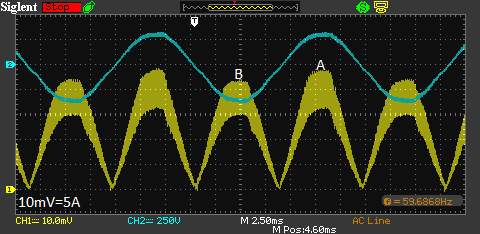
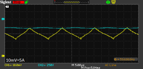
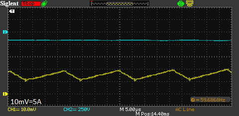
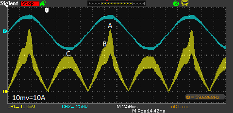
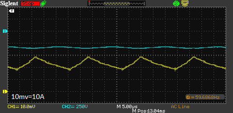
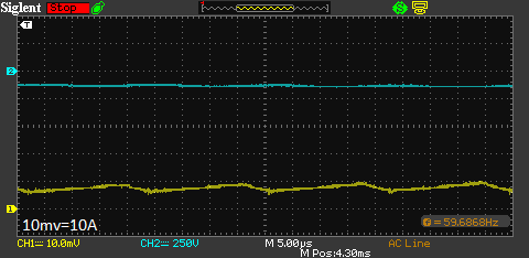
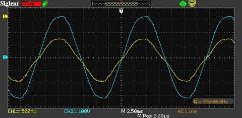
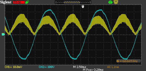
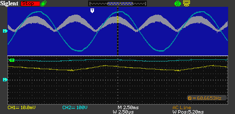
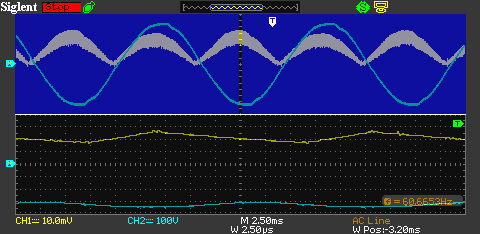
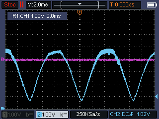
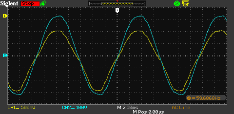
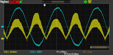
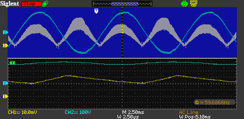
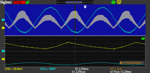
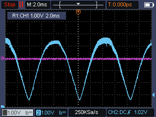
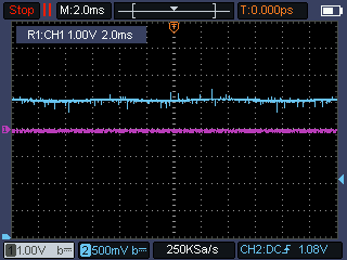
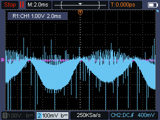
The following thread was closed erroneously. The last post I posted was related to the original topic, TIDA-00779 using the UCC28180 controller. 

e2e.ti.com/.../ucc28180-distorted-input-current-waveform

The last post was:

Prodigy 80 points

Ulrich,

I managed to find the cause of unstable VOUT.  I changed all the components back to original spec for 390V VOUT.  At this point I still had a large difference in VOUT under load.  I then removed my capacitor bank from the board and swapped in the original capacitors.  This resolved the VOUT discrepancy.  Unloaded PFC measured 392V while loaded PFC measured 391V.  

The capacitor bank I used consisted of two of capacitors tied together in series to increase the voltage rating and then I strung a number of these series capacitors in parallel to increase the combined capacitance.  I don't know why this created the issue I was experiencing other than the capacitor bank was located too far from the TIDA-00779 controller (roughly 6") or maybe during one of my earlier failures, a capacitor or two in the bank failed causing these issues.  

I would like to try increasing VOUT again but I will need to swap out the original spec capacitors for higher rated ones.  Should I limit the number the number of capacitors used to increase VOUT stability?  I was thinking of buying 2 x 400V, 5100uF capacitors and tying them in series to yield 800V, 2550uF and attaching the negative terminal of one capacitor directly to the board to minimize distances.  Let me know if this sounds reasonable.

Regards,

  • Hello StnGgc, 

    I think that either two series-connected 5100uF caps or an even number of lower-value series-connected caps (which may or may not be less expensive) can work, provided that:
    a) the connection distances to/from the cap bank is kept as short as possible and
    b) there are parallel resistors attached that keep the voltage stress across each series cap balanced close to 1/2*Vout.  

    I think maybe in your previous implementation there was too much wiring to the cap bank which may have added inductance and facilitated some form of loop instability.   
    I don't think that the absolute number of caps is an issue.  I think it is more important to minimize parasitic components (such as R and L) in your cap-bank structure. (This does not include parallel R's needed for voltage balancing.) 

    Regards,
    Ulrich

  • Ulrich,

    I noticed some waveform distortions when a higher load is suddenly applied under PFC.  (The output voltage is set at 370VDC for now)  It quickly corrects as the sine waves continues.  Is this typical?  Is there is a way to reduce the sudden load distortion?

    Regards,

  • Hello StnGgc, 

    This behavior is typical and normal any time that the boost-PFC output voltage is lower than the peak of the input voltage.  
    When you apply a heavy step load after running at no-load, the voltage loop is slow to respond (as is usual), and the load draws down the output capacitor voltage until the V-loop can increase VCOMP high enough to deliver sufficient power to restore Vout to regulation.  

    Since the boost-PFC has no control over the inductor current when Vin > Vout, you will get that peak-charging distortion until Vout increases.

    Ways to stop it, separately or together:
    1.  Don't increase load so fast.  Depends on your load's flexibility. 
    2.  Increase Cout value.  Adds cost and size. 
    3.  Increase Vout setting.  Increases headroom to the peaks, increases stress to down-stream DC-DC. 
    4.  Speed up voltage loop response.  Increases steady-state distortion.  

    Regards,
    Ulrich 

  • Ulrich,

    I have modified the TIDA-00779 with two 5100uF capacitors tied in series to increase the rated voltage of the system.  I ran it through a series of trials at 392V and it worked as expected.  I then changed a few components to increase the output voltage to 472V.  It works as expected until I overshot the rated loading of 3750W (wattage load used in the excel design sheet).  At 4200 watts, the PFC current waveform seemed to shift downward.  Please see the attached picture.  It this expected when the board is overloaded or is this some other issue?

    Regards,

  • Hello StnGgc, 

    It is neither expected nor normal for the AC input current to "shift downward" in a manner that resembles having a DC bias when the PFC is overloaded.

    However, the screenshots above show CH1 at 500mV/div and the "zero reference" marker is up along the top of the screen, which means that your measurement does not appear to be from a normal current probe. 
    It appears to be from an amplifier of some sort with a DC bias on its output.  

    I would suspect this current probe to be causing the downward shift before suspecting the actual current of acquiring a DC bias. 
    Please investigate how your current measurement is being done and ensure that it faithfully reproduces the actual current waveshape at all current levels without adding any artifacts when the level changes.  

    For a check, I suggest to monitor the boost inductor waveform (preferably with a normal current probe) and compare it to the AC input.
    If the inductor current half-sines are identical each half cycle, then the offset seen in your AC input current above is not real, but a problem with the probe.    

    On the other hand, if the inductor current shows alternating higher and lower peaks on the half-cycles, then some interfering signal must be getting into the ISENSE or ICOMP signal, or even into VCOMP.  Such a signal would have to be synchronized to the full AC cycle and may appear as a repetitive step change in the average voltage on one or more of these pins. 
    I this case, you'll have to find the source of this step-signal and eliminate it, or minimally, prevent it from affecting the PFC control signals.   

    Regards,
    Ulrich 

  • Ulrich,

    I wanted to rule out the amplifier causing the DC bias on the current signal so I swapped out the amplifier circuit for a current transformer.  The current transformer shows a tail forming at the negative peak of the current signal.  Does this give you more information?  If not, let me know and I'll make some modifications to get the current signal after the inductor.

    Regards,


  • Hello StnGgc, 

    Thank you for trying an AC current probe.  IT does provide a little more information, although mostly it simply adds a new "wrinkle" to the issue. 

    Since this current is at the AC input to your system, I cannot be sure that all of the this current is going into the UCC28180 PFC converter or if some of it is going to another circuit connected in parallel to the PFC.  Do you have anything else running off the AC input besides the PFC converter? 

    The upper screenshot shows what could be peak charging into some kind of half-wave rectified circuit.  
    It only shows 3 cycles.  Does this condition persist indefinitely (while in a steady-state line and load condition)? 

    The lower screenshot shows more egregious distortion than your pervious one using the amplifier circuit.  Unfortunately, it doesn't help me diagnose the problem. 

    I think it is important to capture the actual switching current within the PFC inductor. 
    Also, please capture the ISENSE, ICOMP and VCOMP signals as I had requested earlier. 

    Regards,
    Ulrich

  • Ulrich,

    The current displayed is measured just before the UCC28180 PFC converter.  There is nothing connected to the AC input after the current sensor other than the PFC converter itself.

    Yes, the condition does persist indefinitely while in steady-state line and load condition.

    The initial screen shots were taken using a shunt/amplifier circuit as you assumed.  The second set of screen shots were taken using a rudimentary current transformer.  The reason why the second set of screen shots show more egregious distortion is because current readings were exceeding limits of the shunt/amplifier circuit.  The amplifier was clipping the tail section that became visible using the current transformer.  The current transformer shows a more accurate representation of the current signal although the phase angle error is increased relative to the shunt/amplifier circuit.

    Attached below are the screen shots I was able to obtain.  I tried to capture the VCOMP signal but probing the pin caused Vout to shoot up from 472V to over 500VDC when unloaded.  I wasn't comfortable applying loads under these conditions so I wasn't able to obtain the VCOMP signal. 

    I've attached two set of data for comparison purposes.  The first set of signals are taken at 2900watts and the second set are taken at 4200watts. At 2900watts, the input current signal looks good but at 4200watts the above-mentioned distortions appears.   

    2900 watts Vin and Iin 

    2900 watts Vin and ICOMP

    2900 watts Vin and Inductor Current

    2900 watts Vin and ISENSE

    4200 watts Vin and Iin

    4200 watts Vin and ICOMP

    4200 watts Vin and Inductor Current

    4200 watts Vin and ISENSE

    Regards,

  • Hi,

    We will need some time to get back to you.

    Thanks

  • Hello StnGgc,

    I am having difficulty believing any of the CH1 waveforms that you are displaying.   
    I believe the CH2 waveform of AC input voltage using a differential probe. 

    Starting with the 2900W set: 
    a)  Iin looks okay, apparently with a AC current probe.  Minor issues: the pos and neg halves are not symmetrical about the zero-reference line (which is not  actually on a graticule line), and the scale is 2V/div which does not tell me the A/div.  Please include the V to A conversion in such cases. 
    b)  ICOMP signal looks okay, except that it is inverted.  And the zero is not on a graticule line, which sometimes makes measurements a little more difficult. 
    c)  The inductor current is not right, is AC coupled, and shows no switching activity.  I infer that you are using literally an AC current probe rated for 50/60Hz current.  I recommend to obtain a high-bandwidth (30MHz < BW < 200MHz) DC-current probe (such as one from this Tek site: https://www.tek.com/en/products/oscilloscopes/oscilloscope-probes/current-probes )  Make sure it can measure DC currents.  Can be from vendor other than Tektronix; they are just an example.  You can't see switching currents using an low-freq AC probe. 
    I would expect the inductor currents for each half-AC cycle to be identical with the previous and the following ones.  No offsets or asymmetrical lobes (unless the rectified AC voltage has those same offsets and lobes). 
    d)  ISENSE doesn't look right.  It has a shape similar to what is expected, except inverted and offset negative.  There is a lot of noise on the signal.  I suspect this waveform is taken using a differential probe.   

    For 4200W set: 
    a)  The Iin waveform is more distorted, but I think using a 60Hz AC probe masks some details.  The negative half-distortions I think may be due to inductor saturation.  I'm not sure why it isn't symmetrical each half-cycle. 
    b)  ICOMP shows a flat spot at the peak every other half-cycle, probably corresponding to the peaky negative half-of the AC input current. 
    The flat level is at 6V which is an internal clamp level on ICOMP voltage.  When ICOMP is clamped to 6V, the IC loses much control over the current shaping, except for over-current protection.   To eliminate the clamping at 6V, you need to reduce the current-sense resistor (Rs) value.  I'm not sure by how much.  It depends on what your targe maximum power level is.  Be aware that lower Rs allows higher peak inductor currents and if your inductor is saturating, this will only make the saturation worse.  
    The inductor should eb designed to not saturate at the highest peak current at the highest operating temperature. 
    c)  Inductor current looks even weirder and I think the AC current probe simply can't handle the actual current waveforms.  A suitable DC current probe can solve this measurement problem so you can see what the inductor current actually looks like.  
    d)  Same issue with ISENSE signal as a the 2900W level. 

    Normally, probing VCOMP should not affect the PFC operation, but it depends on how you probe it.  If you are using a HV differential probe on the signal, it is probably injecting low-freq noise into the signal causing the Vout variations.  I use a normal 10X scope-probe on VCOMP without issue, but this only works when the AC input source is isolated from Earth-GND.   Essentially, the probe GND-clip connects the PFC GND (the controller GND) to the oscilloscope GND with is earth-GND.  The AC source must be isolated from GND or else it will blow up the circuit.  This can be done using an isolated electronic AC source or by using an isolation transformer in series with the building AC power.  You'll probably need an isolation-transformer rated for 10kVA, which is sizable. 
    Note: a Variac is not isolated!  
    Note also: once the scope is GNDed to the PGND of the PFC, all voltage probes on the scope should have their GND clips tied to the same PGND net.  The GND clips cannot go to different voltages or nets. 

    Regards,
    Ulrich

  • Ulrich,

    Yes, I was using a differential probe to measure both sets of data.  I checked my oscilloscope settings, and I accidently left the "Invert" function on for CH1.  This is why CH1 signals are inverted.

    I ordered a current probe and I'm awaiting delivery.  I'll make the measurements when I receive it.  

    I will also order a 10+kVA isolation transformer but that will take some time.

    In the meantime, I tried using a battery powered oscilloscope and was able to probe Icomp, Vcomp and Isense.  I've attached them below. (Please ignore the magneta horizontal line, I can't figure out how to remove it)

    2900watts Icomp

    2900watts Vcomp

    2900watts Isense

    4200watts Icomp

    4200watts Vcomp

    4200watts Isense


    Do these charts shed any light on the Input current distortions at 4200watts?

    I was thinking of reducing the Rsense value first to see if it eliminates the Input current distortion.  If it makes distortions worse, then I will redesign my inductor for a higher inductance value as you suggested above.

    Regards,

  • Please give us some time to respond to you.

  • Hello StnGgc,

    Thank you for the additional waveforms.  
    Looking at the 4200W ICOMP, it looks almost the same as the 2900W ICOMP except the amplitude is a bit higher which is expected. 
    Each half-cycle of ICOMP looks fairly smooth, and ICOMP is an integration of ISENSE, and ISENSE is a measure of the inductor current, so if ICOMP is smooth (ignoring the switching noise), then I expect the actual AC current to be smooth.  
    Therefore, I am beginning to doubt that the 4200W AC current shape is really as distorted as seen in your earlier posting of "4200 watts Vin and Iin" screenshot.  I really distrust that AC current probe.  By the way, I still would like to know what the A/V scaling is for those screen shots. 

    I can't wait for you to receive your new DC current probe!  It is vital to check out the inductor switching currents, to verify that it is not saturating. 

    Meanwhile, you've got to get rid of all that switching noise on your low voltage waveforms.  
    Comparing 2900W ISENSE to 4200W ISENSE, they look the same.  Given the ~8V pk-pk envelope, the real signal is entirely obscured by switching noise.
    Here is a link to an article about tip & barrel probing to eliminate the noise pickup: 
    https://www.electronicspecifier.com/products/power/oscilloscope-probing-techniques-for-measuring-power-supply-ripple
    It's probably worth setting the channel bandwidth limitation to 20MHz.  For most of the signals, you won't need higher bandwidth. 

    For ICOMP please use 1V/div, same as for VCOMP.  For ISENSE, use 100 or 200mV/div. 
    For the sweep speeds, you see a big picture at 5ms/div, but get more detail at 1 or 2ms/div.   100-200kSa/s is fine here.
    For switching waveforms, you'll be at 2-5us/div.   At these sweeps you'll need 4-8ns/Sa or 125-250Sa/s sample rate. 

    Once you get the isolation transformer in, you'll be able to use a regular scope with earth-GND on the probe barrels. 
    That will provide the cleanest signals.  
    A battery powered scope gets around the non-isolated source issue, but now the whole scope is flying up and down with the AC voltage and that does affect the signals to some extent.  

    Once the input is isolated, your regular scope will nail the PFC section PGND solidly to earth-GND and all the signals will be referenced to a non-moving voltage.  Input isolation is your probing and safety friend.  Just remember that all the probe GNDs have to connect to the same net so as not to short two nets together through the scope. Ideally, all your probe GNDs go to the same point so that you have a common reference for all signals, and ideally that common reference node is the GND pin of the controller IC (although sometimes that much rigor is not necessary). 

    Regards,
    Ulrich

  • Ulrich,

    The scale factor for the current transformer used above is 1V=5A.

    I received the current probe and re-ran inductor current measurements at both 2900watts and 4200watts.  They are attached below:

    2900watts, Channel 1: Inductor Current , Channel 2: Vin

    2900watts, Region A

    2900watts, Region B

    4200watts

    4200watts, Region A

    4200watts, Region B

    4200watts, Region C

    I will re-run the Icomp, Isense, and Vcomp at the settings you suggested above but I don't have an isolation transformer yet so it's still going to be a very noisy signal.

    Regards,

  • Hello StnGgc

    I'm sorry for my delayed response.  I could swear that I replied to you last Friday, but I don't know what happened to it. Maybe I'm just having deja vu, but I remember expressing happiness that you got some real inductor current waveforms, and hoping that your iso-xfmr arrives soon.

    Anyway, the inductor currents at 2900W and 4200W prove that the AC input distortion is real, if you imagine an average current through the middle of the inductor ripple current.  In both cases the half-cycles are asymmetrical; not so much at 2900W, but obvious at 4200W.  The cause of this asymmetry is unknown.  The input voltages at these currents are not so distorted.    

     But we did see that in the ICOMP voltage previously, where the ICOMP flattened out at the 6V clamp level every other half-cycle at 4200W.  

    Try reducing your current-sense resistor value by 10~20% to see if the 4200W distortion reduces or goes away. 
    Again, I don't know why it would be asymmetrical, but the 6-V clamping is one issue and the asymmetry is another, in my opinion.  
    Lower Rs should reduce Vicomp which should avoid the 6V clamp. 

    Regards,
    Ulrich

  • Ulrich,

    I reduced my current-sense resistor value from (0.010/3 = 0.003ohms) to (0.008/3 = 0.0027ohms).  The distortion is gone but the input current waveform is shifted down from the x-axis.  The following is a summary of my findings.  (I also utilized the barrel & tip method to acquire the Isense, Vcomp and Icomp signals.)

    2900watts Vin and Input Current

    2900watts Vin and Inductor Current

    2900watts Vin and Inductor Current Max


    2900watts Vin and Inductor Current Min

    2900watts Icomp

    2900watts Vcomp

    2900watts Isense

    4200watts Vin and Input Current

    4200watts Vin and Inductor Current

    4200watts Vin and Inductor Current Max

    4200watts Vin and Inductor Current Min

    4200watts Icomp

    4200watts Vcomp

    4200watts Isense

    Regards,

  • Can you please leave your email here? I suggest to have an offline discussion as the thread is getting longer and not useful to the community. 

    I believe you need a dedicated resource to support this kind of debug activities.

    Thanks,

  • Can you leave a company email or university email?

    thanks

  • Steven,

    May I know the project application in the public transportation?

    Thanks

  • Ning,

    I think I may have found the root cause of input current shift on my board.  My suspicion is an unbalanced full wave rectifier caused by the diodes integrated in the IGBT's.  The forward voltage across the +VE and GND wing of the full wave rectifier are significantly lower than the other wings.  I believe half of the AC sine wave is rectifying through the IGBT and not the full wave bridge rectifier causing the input current to shift down.  I'm looking to replace the bridge rectifier and/or IGBTs to force rectification through the rectifier and not the IGBT.  

    I don't think there's a need for an offline discussion. I've removed personal information from my previous posts, and for privacy reasons, I'm not comfortable having that information available on a public forum. I believe it may also violate corporate policy. Could you please delete or edit your previous post to remove my name and industry?

    I do appreciate the offer, regardless.

    Regards,

  • Hello StnGgc, 

    I had been away for a while, and Ning has covered this thread for me.  

    It appears that you have apparently solved the asymmetry issue, with no further postings in ~10 days. 

    I will close this thread. 

    Regards,
    Ulrich