This thread has been locked.

If you have a related question, please click the "Ask a related question" button in the top right corner. The newly created question will be automatically linked to this question.

UCC28180: Distorted Input Current Waveform

Part Number: UCC28180
Other Parts Discussed in Thread: TIDA-00779, UCC27524, UCC27324, , UCC28070

Tool/software:

Hello,

I'm trying to understand what is causing Input Current Waveform distortion on 2 boards I have.  They are both TIDA-00779 designs using the same PCB.  Board#1 is an exact duplicate with the same Mosfet hardware and an output voltage of 390V / 3500W.   (I'm using a slightly older PCB version from the most recent)  Schematic is attached below.

tidrka5 - Schematic.pdf

Board #2 uses the same PCB but instead of mosfets, I'm using Infineon IKW40N120T2FKSA1 IGBTs.  Instead of using UCC27324 drivers in Board#1, I'm using UCC27524 drivers in Board#2.  Board#1 uses 12VCC, Board#2 uses 15VCC to drive the IGBTs.  D1, D2, and D3 diodes in Board#2 are similar to the diodes used in Board#1 but are rated for higher voltage.  Board#2 also uses a Capacitor array with the same capacitance rating to Board#1 but with a higher voltage rating.  

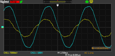
Below are input Voltage and Current curves for Board#1 and Board#2.  The blue line is voltage, yellow is current.  Both voltage and current measurements were measured from a voltage divider and a 0.01R shunt resistor signals passing through isolation amplifier circuits.  

Board#1 @ 1500W - Resistive Load

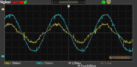
Board#2 @ 1500W - Resistive Load

My intention was to trial running higher output voltages on Board#2 to around 650VDC but I'm noticing input current distortion issues even at 390VDC output voltages.  Both Board#1 and Board#2 exhibit the same distortion but it is much more pronounced in Board#2 than Board#1.  I would like to resolve the distortion issue before I continue testing at higher output voltages.  

Regards,

  • This is the Board#1 Waveform @ 1500W - Resistive Load.  

  • Attached below is another capture take of Board#1 @ 1500W using a current sense transformer.  Voltage measurements here were taken using a differential probe

  • Hello StnGgc,

    As I understand this, the main difference between the two boards is the MOSFETs + drivers, vs. IGBTs + drivers.  Test conditions are the same.

    I attribute the slight difference in THDi to slight differences in turn-on and turn-off timing of the MOSFETs vs. IGBTs. 
    Possibly there is also a contribution from differences of output diodes due to the higher ratings in the IGBT design. 

    I suggest that, although detectable, there is not enough significant difference in the current distortion (in my opinion) to prevent you from raising the output voltage of the IGBT design.   

    To limit risk of severe unexpected current distortion, I suggest increase the Vout setting in small increments, such as 25V or 50V, instead of jumping directly to 650V, and see how the input current behaves.  At each increment, you can gain confidence that the next increment will also behave correctly.

    Regards,
    Ulrich 

  • Ulrich,

    Yes, I was going to bump it up by 50V increments until I reached 650V.

    Ok, if the output current for Board#2 looks satisfactory, I'll continue with my trials.

    Thanks for the feedback.

    Regards,

  • Ulrich,

    I set the output voltage target on my TIDA-00779 board to 475V.  I managed to get up to 3000W output when suddenly it blew up.  I think the root cause was a shunt resistor that I used to monitor the Mains input current overheated and suddenly failed while it was drawing 3000W under PFC.  This resulted in destroying a number of components on the board. 

    Before it blew up, it was regulating the voltage to around 473 volts after the incremental load steps were applied with the PFC on. The output voltage varied from 470V to 474V with 0W to 3000W load applied.

    I rebuilt the board and the PFC works but it doesn't regulate the voltage as well as it used to.  The output voltage under 0W load is 473volts.  At 700W, the output voltage settled to 490V (using a CVSENSE capacitor of 1000pF as specified in the excel calculator).  

    I changed CVSENSE resistor to 820pF and the output voltage settled to 484V at 700W load.  At 0W, the output voltage is still 473volts.

    I changed the RVCOMP and CVCOMP to be more closer to what is specified in the excel calculator and it didn't make any difference.  At 700W, the output voltage is 484V and at 0W, the output voltage is 473V.

    What could be causing the upward shift in output voltage under load?  Is it possible the UCC28180 is damaged or could some other component affect the output voltage in this way?  Should I further reduce the CVSENSE capacitor value?  (It doesn't really make sense since it was 1000pF before it blew up.)

    Regards,

  • If you need Uli's response, please wait for few days.

    To me, if your board was working (output regulate normally) but the new board doesn't (output not regulate well), then I'd check the waveform at each pin to see if they matches the expectation first. Not sure how much you have done and how much you can share.

  • Ning,

    The current output waveforms look good, almost identical to how they looked before.  I'm going to try and replace the UCC28180 controller with a new one to see if it makes a difference while I wait for a response from Ulrich.

    Regards,

  • I've been playing with variables in the Excel Calculator and duplicating them on the TIDA-00779 board in hopes of improving the output voltage swing.  I've been able to reduce the swing in some cases but even in the best case scenarios, the overall swing still seems excessive to me.  The board idles at VOUT(MIN) with no load but when partially loaded (I've been using 600W loads to run these trials) the output voltage hits VOUT(MAX) or higher in some cases.  It doesn't try to regulate the voltage to a constant value.  Attached are my results for Iteration #2 (Before the board blew up with a 473 voltage setpoint)

    Resistance (Ohm) No PFC Voltage (V) No PFC Current (A) PFC Voltage (V) PFC Current (A)
    1900ohms 305.4 0.16 473.5 0.249
    1400ohms  311.3 0.221 473.4 0.338
    900ohms 308.4 0.342 473 0.526
    400ohms 296.1 0.775 471.3 1.198
    341ohms 333.3 0.978 472.5 1.399
    301ohms 333 1.104 472.4 1.574
    260ohms 332.2 1.275 470.7 1.825
    207ohms 331 1.598 473.8 2.293
    154ohms 329.8 2.118 473.7 3.057
    105ohms 329.8 3.11 472.8 4.495

    Strangely enough, at a 390V setpoint, the voltage decreased with increasing load before the board blew up (Iteration#1)  

    Resistance (Ohm) No PFC Voltage (V) No PFC Current (A) PFC Voltage (V) PFC Current (A)
    1900ohms 316.1 0.166 392.4 0.205
    1400ohms  313.5 0.223 392.5 0.279
    900ohms 307.6 0.342 392.2 0.437
    400ohms 298.8 0.75 390.8 0.992
    341ohms 297.9 0.873 391 1.158
    301ohms 296.2 0.984 390.7 1.312
    260ohms 286.5 1.099 391 1.516
    207ohms 327.5 1.58 390.3 1.902
    154ohms 326.1 2.097 388.7 2.526
    105ohms 322.9 3.047 386.3 3.708
    76ohms 329.5 4.304 384.9 5.138
    53ohms 326.7 6.114 383 7.34
    49ohms 326.1 6.55 382.7 7.9

    The following are VOUT results only at 600W load (Iteration#2b to Iteration#2h are after the board blew up and was rebuilt)

    Parameter Component# Iteration#1 Iteration#2 Iteration#2b Iteration#2c Iteration#2d Iteration#2e Iteration#2f Iteration#2g Iteration#2h Units
    P OUT(MAX) 3500 3800 3800 3800 3800 3800 3800 3800 3800 W
    VOUT 390 475 475 475 475 475 475 475 475 V
    RISENSE R11 220 220 220 220 220 220 220 220 220 Ohms
    CISENSE C15 2700 2700 2700 2700 2700 2700 2700 2200 2200 pF
    RFB2(actual) R9 13 10.5 10.5 10.5 10.5 10.5 10.5 10.5 10.5 kOhms
    CVSENSE C11 820 820 1000 820 1000 820 820 820 820 pF
    CICOMP(actual) C10 3300 3300 3300 3300 3300 3300 3300 3300 3300 pF
    CVCOMP(actual) C14 8.2 8.2 8.2 8.2 10 8.2 8.2 8.2 8.2 uF
    RVCOMP(actual) R10 10 15 16.9 16.9 13.7 15 13 13 13 kOhms
    CVCOMP_P(actual) C13 0.39 0.39 0.22 0.22 0.27 0.27 0.39 0.39 0.39 uF
    RSENSE R4, R5, R45 0.003 0.003 0.003 0.003 0.003 0.003 0.003 0.003 0.005 Ohms
    PFC Voltage 473V 490V 484V 492V 488V 486 486 490

    Attached is my excel calculator for your reference.

    UCC28180 Design Calculator TIDA-00779 - sluc506c.xlsm 2bnd Iteration.xlsm

  • I have informed our local FAE to contact you regarding this project. We can have a meeting to discuss this more efficiently.

  • Hello StnGgc,

    Variations of output voltage with load are not caused by any of the components that you experimented with in your iterations. 

    The usual cause of such Vout variations are:
    1.  Noise injected into the VSENSE net; can make VOUT go up or down.
    2.  Board-surface leakage-current around the high-value feedback resistor(s) (RFB1) from VOUT to VSENSE; makes VOUT go down.
    3.  Other kind of leakage-current around the lower feedback resistor(s) (RFB2) from VSENSE to GND; makes VOUT go up.

    4.  TIDA-00779 has a 4th possibility from its boost-follower control circuit; more or less current through Q4 affects VSENSE.  Less collector current makes VOUT go down.  
    High power output can heat up the board.  This heating up can reduce Schottky diode D8 forward drop, making Q4 base voltage go down which makes Q4 collector current go down which makes VOUT go down. 

    I recommend to debug your board(s) to work first without the boost follower circuit. Remove Q4 during this debug. 
    After your PFC works at max power and highest VOUT, then start to consider how the Q4 circuit will interact with the VSENSE and affect your VOUT.   

    Regards,
    Ulrich 

  • Ulrich,

    After playing around with the components listed above, I figured it must be noise affecting VSENSE as you mentioned in your response.  I took my first baseline TIDA-00779 board (equipped with mosfets) and changed out the capacitors to a higher rated capacitor bank and RFB2 from 13K to 10.7K.  The output voltage increased from 390V to 472V as expected.  Under 600W load, the output voltage only dropped from 472V to 470V (as opposed to increasing to 485V+ on the IGBT board).  To try and figure out what is causing noise on the IGBT equipped board affecting the VSENSE signal, I've swapped out the lower rated diodes for higher rated diodes and didn't notice any issues at 600W load.  Later today, I plan on swapping out the mosfets for IGBTs to see if they are the source of noise.  It must be something because both boards are the same except for the mentioned diodes, IGBT driver and IGBTs/Mosfets.  

    I do notice quite a bit more noise on oscilloscope Voltage/Current signals testing on the IGBT board vs the Mosfet board.

    I don't have any of the boost follower circuit populated. I'm only using fixed output configuration.

    Thanks for the feedback/suggestions.

    Regards,

  • Hello StnGgc,

    I don't know what would make IGBTs noisier than MOSFETs, but a well laid-out board should not be susceptible to either of them. 

    I suggest to look for current-circulation loops where high switching currents could magnetically couple noise into the VSENSE network, or overlapping tracks or planes with high switching voltages which could capacitively couple noise into the VSENSE network.

    All current loops should be minimized in loop area as much as practicable, and switching voltages minimized in overlap area as much as practicable.
    Also, high GND currents should be routed in separate paths to stay out of the "quiet" GND of control signals. 

    Regards,
    Ulrich

  • Ulrich,

    I've been trying a number of different things to improve Vout stability under different loads.  I have swapped out the IGBT's for Mosfets because the higher Vbias voltage used for IGBT's increases Vout variation under different loads.  With a lower Vbias (using mosfets) I'm able to improve Vout variation.  There is still a relatively high amount of variation, but it's less than when I used IGBT's.  

    Another thing I have noticed is that VCC (with PFC on and no load applied) measures 11.89V using a mulitmeter.  When a load is applied with PFC on, VCC gets pulled down to 11.7V.  I'm not sure if this affects anything from a control standpoint, I though I'd mention it.

    Also, Vsense measures 5.009V with PFC on and no load applied.  Vout measures 472V.  When the load is applied with PFC on, Vsense measures 5.049V and Vout jumps to 480V.  Shouldn't the controller see this higher Vsense value and attempt to adjust Vout down to 472V?  (The measurements were taken from TP10 and TP8.)

    Given the existing TIDA-00779 PFC design as outlined in PCB layout TIDRKA8, If I were to move R6, R7, and R8 as outlined in the attached drawing, would I notice Vout stability improvements by moving the voltage divider resistors closer to the UCC28180 controller?

    Regards,

  • Hello StnGgc, 

    I don't think the variation of VCC is significant, nor contributes to the regulation problem. 

    I do think that the three resistors of the upper feedback network should definitely be moved down close to the controller.
    The long path between where they are located now and the controller VSENSE input is the VSENSE signal and that can pickup lots of switching noise. 
    Noise which gets worse as load power increases, because switching current increases.  
    If this is the way the TIDA-00779 board is laid out, it is a poor layout for VSENSE. 

    The switching noise can fool the controller into "thinking" that the VSENSE voltage is actually regulating at 5.00V by diverting some feedback current driven by the excessive VOUT.  Moving the 3 FB resistors close to the controller changes the noise coupling path to the high voltage output track, where the noise can have no effect.  

    It does mean that the output's high voltage track will travel closer to the IC, so additional spacings may be needed in that vicinity depending on how your actual layout looks. 
    Another option is to move switching tracks away from the FB path, which may be a bigger redesign effort that moving the resistors. 

    Regards,

    Ulrich

  • Ulrich,

    Thanks for the feedback.  I'm going first try moving the 3 resistors closer to the UCC282810 controller by cobbling something together (using the existing PCB for trialing purposes) and compare the results.

    Regards,

  • Ulrich,  

    I've tried moving the resistors closer to the UCC28180 controller but it didn't make any difference.  I think ground noise must be affecting the VSENSE signal on the controller.  I downloaded the latest TIDA-00779 Gerber files and compared them with the version I have.  I noticed in the newer version, a large solid ground plane extends underneath the UCC28180 controller.  The version I have, doesn't have a solid ground plane.  Instead, it has traces and filled zones feeding ground to the various components. 

    Also, the 3 Vsense resistors in the latest version are moved closer to the UCC28180 controller.

    The latest version also has an DC/DC power supply feeding VBIAS voltage to the controller and driver.  

    I'm assuming the changes between these two versions were made to help keep noise interference to a minimum.  Do you think the latest PCB version will help resolve unstable VOUT voltages?  

    Attached are the differences between the two.


    (I also tried populating components for the Snubber Circuit R28, C21, but that only made the VOUT swing greater when under load and unloaded.)

    Regards,

  • Hello StnGgc, 

    I imagine the newer layout is some improvement over the previous one, but I do not know how much better. 

    I am not impressed with either of them, based on the fact that I can see two switching MOSFETs laying down over the UCC28180 control and gate-drive circuitry.  This allows the MOSFET drains high-voltage switching voltage to capacitively couple into the control signals, including the VSENSE net.

    The newer layout may or may not have the local GND plane extended and positioned between the MOSFET drains and the circuitry.
    I don't know what the layering stack-up is, but even if the GND plane is between them, it may only attenuate the switching noise, not block it completely. 
    If there is a grounded heatsink between them, maybe that helps, but I can't tell from the limited layers shown. 

    In any case, I recommend that you lay out your own pcb using sound design principles to minimize switching loop areas, minimize dv/dt coupling, and keep control-signal GND return paths separated from the switching-current power GND return paths.   
    A good design will not have any significant Vout swing.

    Please refer to this app-note on the subject.  Although it is targeted for dual-interleaved PFC, its basic principles can be adapted for a single-phase boost PFC as well.  https://www.ti.com/lit/pdf/slua959

    Regards,
    Ulrich

  • Ulrich,

    I'm currently designing a multi-leafed power supply using the UCC28070 controller.  I was going to use the TIDA-00779 power supply (that I currently have) as a "springboard" to a higher powered rated power supply.  Would it be possible to discuss/review my design offline via email?  I can't share details publicly.  

    Regards,

  • Hi StnGgc, 

    Unfortunately, with limited "bandwidth" available, I can't afford the time to be a personal consultant on PFC design. 
    The main purpose of these E2E forums is to allow other engineers to learn about common issues and solutions involving all sorts of TI controllers. 

    There are not many aspects of PFC design or schematic that are not already wide-spread in the public domain, unless it involves special proprietary circuitry concerning some limited detail of a design.  In such a case, this special circuitry can be removed or hidden from view while discussing the larger issue.
    Most often, a concern or issue can be discussed in general terms, even with actual waveforms that illustrate the issue. 

    This thread involves unwanted variations of output voltage in a UCC28180 design, which hopefully can be closed out soon.    
    For issues in a new design using the UCC28070/A controller, please start an new thread.  

    Regards,

    Ulrich

  • Ulrich,

    I managed to find the cause of unstable VOUT.  I changed all the components back to original spec for 390V VOUT.  At this point I still had a large difference in VOUT under load.  I then removed my capacitor bank from the board and swapped in the original capacitors.  This resolved the VOUT discrepancy.  Unloaded PFC measured 392V while loaded PFC measured 391V.  

    The capacitor bank I used consisted of two of capacitors tied together in series to increase the voltage rating and then I strung a number of these series capacitors in parallel to increase the combined capacitance.  I don't know why this created the issue I was experiencing other than the capacitor bank was located too far from the TIDA-00779 controller (roughly 6") or maybe during one of my earlier failures, a capacitor or two in the bank failed causing these issues.  

    I would like to try increasing VOUT again but I will need to swap out the original spec capacitors for higher rated ones.  Should I limit the number the number of capacitors used to increase VOUT stability?  I was thinking of buying 2 x 400V, 5100uF capacitors and tying them in series to yield 800V, 2550uF and attaching the negative terminal of one capacitor directly to the board to minimize distances.  Let me know if this sounds reasonable.

    Regards,

  • Hello,

    Please start a new thread for UCC28070 related topics. You can also contact our local FAE to share additional information like waveforms if you are not comfortable to share via the forum.

    Thanks,

    Ning