This thread has been locked.

If you have a related question, please click the "Ask a related question" button in the top right corner. The newly created question will be automatically linked to this question.

TPS6594-Q1: some issues TPS65941213 and TPS65941111 power supply

Part Number: TPS6594-Q1

Tool/software:

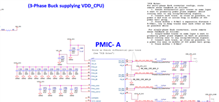
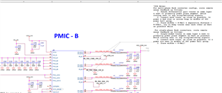
We have chosen the TITPS65941213+TPS65941111 power supply solution, and the following issues arise: 
1. If we design according to the power supply scheme provided in the document "PROC112A1 (001) _SCH" on the official website, the newly purchased TPS65941213 and TPS65941111 chips do not require additional software configuration. Can each power supply directly output normally after power on; If VIN is changed to 5V input, no additional configuration is required when powered on, what is the difference between it and 3.3V input.
2. Do the sampling points FB1 and FB2 of PMIC-A and PMIC-B in the figure have to be located below SOC as given in the document, and do they have to be pseudodifferenced.

PROC112A1(001)_SCH.pdf

  • 1. If we design according to the power supply scheme provided in the document "PROC112A1 (001) _SCH" on the official website, the newly purchased TPS65941213 and TPS65941111 chips do not require additional software configuration. Can each power supply directly output normally after power on; If VIN is changed to 5V input, no additional configuration is required when powered on, what is the difference between it and 3.3V input.

    Please see the User's Guide, https://www.ti.com/lit/ug/slvuc99a/slvuc99a.pdf?ts=1747317996814

    The system is not 100% independent of software, feature such as low power modes, SD_CARD voltage, or etc... may require software to write over the I2C bus to enact changes.

    A power up and down of the system can be done without software, but the full feature set requires software which is bundled with the appropriate SDK for the processor depending on OS (RTOS, LINUX, or baremetal).

    As for changing the voltages during runtime, yes that is possible, it's called Adaptive Voltage Scaling (AVS).

    The PDN is made for an input of 3V3, some of the LDOs on the PMIC act as load switches for optimization with an expectation for 3V3 any input outside of these  preprogrammed thresholds will result in an error upon power up.

    See Table 3-3. Digital Connections by System Feature & Table 3-1. PDN Power Mapping and System Features on features that can be removed for any changes as according to the above User's Guide.

    2. Do the sampling points FB1 and FB2 of PMIC-A and PMIC-B in the figure have to be located below SOC as given in the document, and do they have to be pseudodifferenced.

    Yes, they do. This is requested as best practice to avoid noise and to get the best accurate read of the true voltage at the point of load, while under smaller current draws this may not be an issue, but under worst case conditions could this be problematic.

    One thing that the PROC schematic may not have mentioned if that there is ferrite beads/chokes from the point of load nets, have the feed back traces go before the in series choke. This additional request is due to the additional parasitic parameters as well as the unaccounted for inductance that the ferrite introduces to the feedback loop.

    BR,

    Nicholas McNamara