Tool/software:
Hi,
In our application, the load current is 3 A and the expected VSYS voltage is 16.8 V, resulting in an output power of approximately 45 W. In this case, would it fall within the Safe Operating Area (SOA)?
Best regads
Akin
This thread has been locked.
If you have a related question, please click the "Ask a related question" button in the top right corner. The newly created question will be automatically linked to this question.
Tool/software:
Hi,
In our application, the load current is 3 A and the expected VSYS voltage is 16.8 V, resulting in an output power of approximately 45 W. In this case, would it fall within the Safe Operating Area (SOA)?
Best regads
Akin
Hi Alan,
Thank you for your response.
In the absence of VBUS, if the battery voltage is at 12 V and the system load draws 3.9 A, would the charger IC still be able to operate under this condition? Specifically, can it supply sufficient power to the load directly from the battery?
Looking forward to your clarification.
Hi Alan,
Thank you for your clarification.
I have a follow-up question regarding the input source. If the VBUS input voltage comes from a source similar to a battery output charger, where:
In one condition, the source provides 12 V at 3 A, and
In another, it provides 15 V at 1.6 A,
And the device’s system load requires 16.8 V at 3 A, then the device needs to boost the input voltage to meet this requirement.
Could you please clarify how much current can be delivered at 16.8 V output in both of these input conditions?
An attached block diagram is provided for better clarification.
Looking forward to your response.
Best Regards
Akin
Hi Akin,
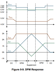
The total current can be provide assuming there is a charged battery at the device output. When source is 12V*3A=36W*, the 16.8V*3A=50.4W load will pull 50.4W-36W* = 14.4W from the battery. The SYS voltage drops to the battery voltage in this case and follows the battery voltage down. The * indicates that the output from the source has some losses that I ignored so it will provide less than 36W on it output and pull slightly more from the battery With 15V*1.6A = 24W source, even more power comes from the battery. A simplified diagram of the power path response is shown below:

Regards,
Jeff
Hi Alan,
Thank you for your clarification.
If we configure the device’s battery charging current to 1.3A, and consider the same scenario as before, I have a follow-up question:
Under these conditions, can the device still provide 50.4W at the output? Specifically, will the VBUS be able to supply the 36W and the battery can supply 14.4W, considering the charging current limit?
Looking forward to your insights.
Regards
Akin
HI Akin,
The charge current must be set high enough to recharge the battery in between 50.4W output load pulses or the battery will eventually become fully discharged. When the battery is discharging, the charge current setting is irrelevant. V(SYS) = V(BAT) and the battery discharge current feeds the load.
Regards,
Jeff
Hi Jeff,
Thank you for your clarification.
If our system load is 16.8 V @ 3.13 A (52.584 W) and the input power is 30 W, could you please help us understand the power dissipation of the charger IC in this scenario, ideally in watts?
Appreciate your support.
Regards
Akin
Hi Akin,
52.584W - 30W*efficiency must come from the battery. So, assuming efficiency is 100%, 22.584W must come from the battery. If the battery is fully charged at 16.8V, 22.584W/16.8V = 1.34A. The charger internal battery FET must dissipate 1.34A*1.34A*Rdson. So the charger must dissipate 30W (1-efficiency) + 1.34A*1.34A*Rdson. Keep in mind, since the charger is input power limited, V(SYS) drops to the battery voltage and follows the battery voltage as it discharges.
Regards,
Jeff