This thread has been locked.

If you have a related question, please click the "Ask a related question" button in the top right corner. The newly created question will be automatically linked to this question.

UCC28950: Transformer Coupled Gate Drive-Using UCC27324D

Part Number: UCC28950
Other Parts Discussed in Thread: UCC27324

Tool/software:

Hello,

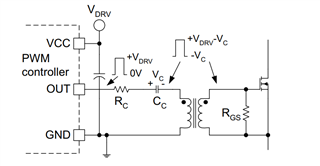
In Picture 1, I put some arrows on the UCC27324D driver, capacitor (C14), transformer (T3) and mosfets (Q1 and Q2) to follow easily on the picture. Application is phase shift full bridge dc-dc converter.

I may have a mistakes in my way of thinking but let me summarise as follows:

When I first look at section that I put arrows on them, I saw C14 capacitor. This capacitor reminds me it removes the DC offset from the signal coming from UCC27324D outputs (OutA, OutB). That means this capacitor will change the signals into something like VoutA-VC14 being high state and -VC14 being low state. Same thing happens to the OutB which is VoutB-VC14 being high and -VC14 being low. (Vc is the voltage on the C14 capacitor.)

UCC27324D IC is given as dual noninverting in it's datasheet which means outputs will follow inputs.

So let me come to the point which makes me very confused as follow:

We know that the input signals of UCC27324D are phase shifted signals coming from UCC28950. We also know that there is C14 capacitor. This capacitor (as I explained it's mission above) will affect the signals coming from UCC27324D in such a way that these signal will have positive half and negative half due to DC offset removal. isn't it? You can see what I mean in the picture 2. I draw an approximate mid line on the signal to show positive and negative half.

Considering these signals (DC blocking is in play), transformer will have one positive from one side (pin 1 of TX) and one negative section from the other side (PİN 2 of TX) at the same time .

Meaning that if I have let's say for simplicity +10V on the pin 1 of TX and -10V on the pin 2 of TX, is this create 20V on the transformer ? or when both of the signals is on the negative half, meaning 0 V across the transformer . Is this how these signals (considering the effect of DC blocking capacitor) work on the transformer ?

Picture 1. The circuit given in the datasheet

Picture 2. The explanation of what I tried to say in the question 

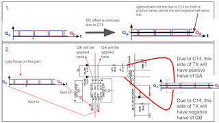
Picture 3. To emphasize what is the effect of C14 capacitor 

  • C14 is a DC current block capacitor to avoid transformer saturation. 

    T3 is a transformer to achieve the level shifting feature to bias both high and low side FET.

    I suggest you to build a RC circuit model and run the simulation to get a good virtualization.

    There are few models you can start with.

    https://www.ti.com/product/UCC28950#design-tools-simulation

  • Hi

    You said mostly what I said in my question. 

    Best regards

  • Does this mean you have no more questions?

  • No, basically your answer didnt contribute almost anything.

    Basically question ask with the given signals and considering the effect of dc capacitor, how these signals operate on the transformer and make the transformer work ? because ıt seems there is a positive halve on the transformer  and negative halve at the same time (points between point 1 and 2 on the ransformer ).

  • Hi,

    The first thing to note is that QA and QB are complementary signals, as you have shown in your second diagram (for simplicity, I am ignoring any dead time between OUTA and OUTB). 

    As you have also said, the UCC27324 is a dual non-inverting driver chip. This means when INA is at a high level, OUTA will also be at a high level.

    As INA and INB are complementary, we know that when INA is high, INB will be low. Therefore, OUTB will also be low.

    As the UCC27324 has totem pole outputs, this means the outputs are driven to VDD and to GND. Therefore, when INA is high (and INB correspondingly low), OUTA is at VDD while OUTB is at GND. When INB is high, OUTA is now at GND, while OUTB is at VDD.

    Measuring thr voltage across OUTA and OUTB, we would see pulses of +VDD and -VDD. Placing a gate drive transformer across OUTA and OUTB as shown in the first diagram would mean the primary of the transformer is driven by +VDD and -VDD pulses.

    As a result, the MOSFETs VGS would also see +VDD and -VDD pulses (although note that the winding polarity for the secondaries are opposite, so one will be driven +VDD while the other will be driven -VDD)

    C14 ensures that there is no DC buildup across the transformer as a result of an imbalance between OUTA and OUTB. As long as OUTA and OUTB are identical (which in simulation, they are of course) - C14 is not required. I have gotten converters to work without a DC blocking capacitor, although I do believe it helps, at least with transient loads.

    This is an easy circuit to simulate, so for a better understanding of the signals + the impact of parasitics, I would recommend simulating the circuit.

    Hope this helps.

  • Hello Sir,

    Thank you for your nice explanations. I have a little bit clear understanding with the help of you.

    But still there is something which itches me still. 

    I added the Picture 3, the same strategy is applied. No difference with Picture 1. The circuit in Picture 3 is also from Texas Instruments.

    So, As you can see in Picture 3, capacitor pulls the drive signal down such that it has some positive and some negative parts. This is the most important part for me to understand the circuit. Why the capacitor (C14) given in Picture 1 is not pulling the signals down  due to DC offset removal as given in the Picture 3 ?

    When I want to integrate this '' pulling down'' action  onto the circuit with C14, the result becomes as I drawn in the Picture 3 in which I draw a midline for the signals, and result becomes false, why ?  

    In summary, why do we have a ''pulling down'' action in Picture 3 and not have in the circuit with C14 ? 

  • The difference between the circuit in Picture 1, and Picture 3, is that in Picture 1, the transformer is placed across OUTA and OUTB, whereas in Picture 3, the transformer is placed between OUT and GND. This means that in Picture 1, the outputs are only +VDD pulses, not +VDD and -VDD pulses like in Picture 3.

    The 'pulling down' effect (where the gate drive signal gets centred such that it has 0V DC component) is simply because it is a unipolar signal (only +VDD and GND), so there is a DC voltage that the capacitor is blocking. 

    In Picture 1, there is no DC voltage, as the pulses are +VDD and -VDD. Therefore, the capacitor is not 'blocking' anything, so the signal across the transformer is unchanged.

  • Ohh, woow sir you can not imagine how happy I am now. I got the point.

    I think you meant to say GND instead of -VDD in your sentence here '' This means that in Picture 1, the outputs are only +VDD pulses, not +VDD and GND pulses like in Picture 3. ''

    Best regards 

  • Glad I could help!

    Apologies I got those two pictures mixed around, it should say: "This means that in Picture 3, the outputs are only +VDD pulses, not +VDD and -VDD pulses like in Picture 1."

  • Sir thank you so much for everthing.

    Apart from topic, I wondered very small point. There are two schottky diode between OUTA /OUTB and GND. The driver is already capable of sink/source of the current in both directions. Why should we place a schottky diode across the outputs ? 

    Best regards

  • As far as I am aware, the schottky diodes prevent the pin on the driver chip from going negative with respect to GND. If the pin has a negative voltage on it, the diode will conduct which will prevent damage to the driver chip. Hope that helps.

  • Thank you for spending time elaborating here. 

    I think the issue is closed.