Tool/software:
Hello
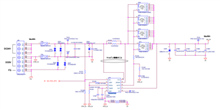
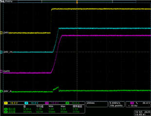
The Enable pin of the TPS2491 is used to control the ON/OFF of 24V DC to the load.
The maximum current of the load is 66A.
I use three MOSFETs, 80V, 310A, 1.6mΩ, in parallel.
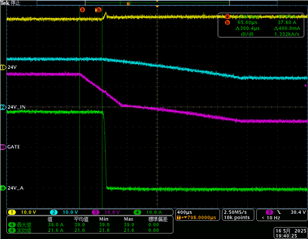
The problem is that when Enable is turned off, the FET burns out.
The questions are listed below.
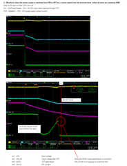
1) Is it correct to use the Enable control while DC 24V is being supplied to turn the power supply to the load on and off?
(Unlike operation with hot plugging and unplugging, is it okay to use Enable control when DC24V is not disconnected?)
2)If the above is not the problem, please tell me the cause and solution. I have attached a circuit diagram.
3)If the TPS2491 cannot be used in the manner described above, please tell me of any alternative devices.
Thanks for the best reguard.