This thread has been locked.

If you have a related question, please click the "Ask a related question" button in the top right corner. The newly created question will be automatically linked to this question.

BQ25504: Glitch in the Functional Block Diagram?

Part Number: BQ25504


Tool/software:

The BQ25504 is neat device that i got running quite well, up to a couple of minor points i do not understand. Before we get to that my first question is if it can be that there is a small error in the functional block diagram presented on page 12 of the datasheet SLUSAH0G – OCTOBER 2011 – REVISED AUGUST 2023 (Revision G), which is the latest version afaik. Here is part of that diagram:

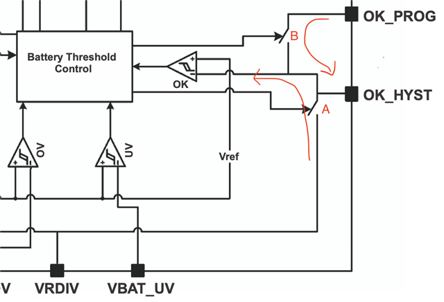
Observe that when internal switch A is closed VRDIV is connected OK_HYST (which seems okay for some measurement mode) but also to the opamp and compared with Vref. Although the latter could serve some function, it seems incorrect here, because it would render the measurement of OK_PROG impossible at the same time. However, the latter is needed in order to determine the value VBAT_OK_PROG, since that formula does not contain ROK3. So, i have the feeling the circuit should be something like this:

Here, if switch B is closed and A is open VBAT_OK_HYST can be determined  and if both are closed, ROK3 is effectively shortened (see below), so that VBAT_OK_PROG can be measured. 

When measuring the voltage over ROK3, this line of reasoning seems to be confirmed. With decreasing voltage VSTORE the voltage over ROK3 is zero, whereas is suddenly becomes positive after passing the VBAT_OK_PROG threshold. But the question remains, what is the role of switch B? So probably i am still missing something here.

Could you comment on my reasoning and the role of switch B?

  • Hello Ruud,

    We are reviewing your questions and will respond by the end of day.

    Sincerely,

    Wyatt Keller

  • Hi Ruud,

    This part has been in production for 14 years and has been functioning as expected. The block diagram does not paint the full description of the part nor is intended to. I believe the connection points for switches "A" and "B" are to both provide the reference for the dividing voltage as well as connect the comparator to the reference setting.

    Regards,

    Mike Emanuel

  • Hi Mike,

    Thank you for looking into my question.

    >> This part has been in production for 14 years and has been functioning as expected.

    Yes, nobody suggested otherwise, I was politely trying to address a possible error in the datasheet. Even after 14 years and 6 revisions it may be that there is room for improvement. Under the assumption my observation is correct of course. 

    >> The block diagram does not paint the full description of the part nor is intended to

    Fair enough, you cannot show every detail in the block diagram. But should the parts that are shown not be a faithful representation of the internal operation? 

    >> I believe the connection points for switches "A" and "B" are to both provide the reference for the dividing voltage as well as connect the comparator to the reference setting.

    Yes, in general this is true, but as drawn it cannot be correct imho. If possible, I would appreciate a more detailed answer, for i have some other findings I don't understand when experimenting with this device and it helps to be confident about the assumptions of the internals first.

    Thank you for your patience. Best Regards, Ruud.

  • Hi Ruud,

    As stated before we cannot include every detail in a block diagram. We appreciate your feedback.

    Regards,

    Mike Emanuel

  • Thank you for your time.