This thread has been locked.

If you have a related question, please click the "Ask a related question" button in the top right corner. The newly created question will be automatically linked to this question.

TPS25730: USB controller not working

Part Number: TPS25730

Tool/software:

Hello, we have implemented your TPS25730 controller in our electronics, but before doing so, we were able to determine its operation by manipulating your TPS25730EVM test kit, configured to supply 20V and a minimum current between 0.5 and 1.5A. To do this, we toggled the switches as follows:

SW5 for ADCIN1: value 4
SW4 for ADCIN2: value 7
SW3 for ADCIN3: value 0
SW2 for ADCIN4: value 3

This allows us to verify proper operation, and therefore 20V.
This is with a 100W charger.

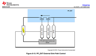
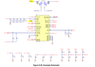
So we took inspiration for our electronics as shown on the supplied components, fixing the divider bridges by referencing your model, but it doesn't work, the measured output voltage fluctuates from 5V to 0V?....
Knowing that there are few external components to do this, what do you think the problem would be? Thank you for your support.

TPS25730 Geeps.pdf

  • In our schematic, we're not using I2C, but we've kept this option. For the moment, R43 and R44 are missing, and R101 and R102 are present.

  • Hi Laurent,

    Thanks for reaching out and sharing your schematic.

    From first glance, it is likely due to leaving the Fault in pin floating. You should bias it high (a weak pullup resistor to LDO3V3) to ensure it is in the "Maintain connection" state.

    In addition, you should have the VSYS pin connected to the PPHV node (the source of the system side fet of Q7) as this is the reference for the GATE_VSYS gate driver.

    Thanks and Regards,

    Chris

  • Hi Chris, and thanks for your reply.

    Yes, indeed, I noticed that the "FAULT IN" pin was floating, so I connected it as a 10K pull-up on LDO3V3, and my constants are indeed more stable now.

    However, I do have 20VDC on VBUS but only 9.1VDC on PPHV, even though I have corresponding fixed voltages measured on the ADCINx:
    ADCIN1 1.0426V
    ADCIN2 3.431V
    ADCIN3 0.0392V
    ADCIN4 0.0392V
    With an LDO3V3 output at 3.46V

    Indeed, VSYS should be at PPHV, and since I'm using the TPS25730EVM as inspiration, it's not present... so I didn't plan to address it, so I must...
    But if I understand correctly, VSYS is only a control for the reverse current and has no influence on the output voltage? This is why I don't understand why I have 9v instead of 20v in PPHV?

    Best regards

    Laurent Ifergane

  • Hi Laurent,

    Because you are using the S (external power path) variant, the VSYS pin is used for biasing the gate driver GATE_VSYS pin. The TPS25730EVM uses the D variant (internal power path) so does not use the VSYS or GATE_VSYS pins.


    I'm not sure why your implementation is only accepting 9-V.

    You have a TPS25730EVM? If you configure it to:

    ADC1: 4, ADC2: 7, ADC3: 0, ADC4: 0

    like your board and connect it to the same adapter, does it also go to 9-V or can it negotiate 20-V?

    I tested your settings with a TPS25730EVM using an adapter I know can negotiate 20-V, and it seems to be fine.

    You are correct, the VSYS pin should not affect the negotiation, it should be set by the ADCINx pins.


    Do you have a PD analyzer? Something that can capture and decode the CC-line messaging? This would be the best way to confirm the behavior as it would show us what the Source is offering and what the TPS25730 is requesting.

    Thanks and Regards,

    Chris

  • Hello Kris,

    yes I use the same charger as for the TPS25730EVM board which negotiates 20v very well.

    And to know that my electronics receive 20vdc which I see of course Vbus so before the MOsfet, so my charger is providing me with 20v ... but after the mosfet I only get 9v?

    Wouldn't Vsys ultimately play a role?

    Thank

    Best regards

    Laurent ifergane 

  • Hi Laurent,

    And to know that my electronics receive 20vdc which I see of course Vbus so before the MOsfet, so my charger is providing me with 20v ... but after the mosfet I only get 9v?

    If I understand correctly, with your board, you do see 20-V on VBUS, but you are dropping 13-V across the FETs?

    Is the 13-V drop shared between the two FETS or is it all on one FET?

    If it is primarily on the VSYS FET, it is likely because you do not have VSYS connected to the source of the FET. As mentioned above, VSYS is used as a reference for the charge pump gate for the GATE_VSYS gate driver. Without this properly connected, I'm not sure how the GATE_VSYS pin will behave.

    Thanks and Regards,

    Chris

  • Hello Chris

    Indeed, I needed to polarize the second MOSFET N via Vsys, which I connected to its source, and it worked.
    I'm getting my 20VDC output.

    Thank you for your help, which helped me move forward.
    Have a nice day.

    Best regards

    Laurent Ifergane