This thread has been locked.

If you have a related question, please click the "Ask a related question" button in the top right corner. The newly created question will be automatically linked to this question.

TPS546D24S: Problem for 4 phase stack

Part Number: TPS546D24S
Other Parts Discussed in Thread: TPSM8D6C24, TPS546D24A,

Tool/software:

Hello 
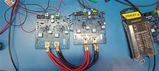
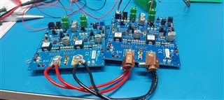
I am facing problems in 4 phase stacking. by using TPS546D24SEVM i was able to do 2 phase stacking now by using 2 TPS546D24SEVM i am trying for 4 phase stacking. i am not getting any communication error as i can see on BCX_CLK and BCX_DAT communication happening with followers. i will explain my setup it is as follows


1.I am using 2 TPS546D24SEVM in that for configuration i am using PMBUS programing not using Pin strapping method storing all values in NVM and doing pin detect override 0x0000.

2.STACK_CONFIG is 0x0003 and INTERLEAVE is 0x0040,0x0041,0x0042,0x0043 for master followed by 3 followers

3.for 2 EVM i am connecting BCX_CLK, BCX_DAT, SYNC, VSHARE and GROUND to each other 

4.To make follower i am making sure that GOSNS pin is connected to BP1V5 by using 10k resistor in EVM that is R8_P1, R8_P2 and in 1st EVM R8_P2

5.i have made sure that VSEL, MSEL1, ADRSEL are all connected to AGND in follower. 

6. for PGD/RST i have removed R26 which is connected to BP1V5. and connected it to PGND as per datasheet

7. VOSNS pin i have connected to PGND in SLAVES


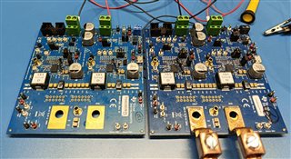
from right side 1st is master and others are follower.
problem i am facing is
1.as when i set voltage for 1 st evm where master is connected voltage setting is correct. but at other EVM voltage is setting higher and its keep on increasing that is why i am getting OVER_VOLTAGE_WARNING error
2.i tried to connect output of both as well together but voltage is getting equalised from left EVM to right one

any more hardware changes are required please let me know.
Thank you for any help suggestion in advance

Thanks 
Parth

  • Hi Parth,

    INTERLEAVE is Read only in a multi-stack configuration and must be pin programmed instead. To program INTERLEAVE, you will need to connect resistors from MSEL2 to AGND. Here are the resistor values you need to install for each phase:

    • For the Phase 00 leader, install 8.25 kΩ resistor
    • For the Phase 02 follower, install 68.1 kΩ resistor
    • For the Phase 01 follower, install 6.81 kΩ resistor
    • For the Phase 03 follower, install 31.6 kΩ resistor

    Also, while the applications note is for the 2-device module, the TPSM8D6C24, we have an applications note describing how to stack two 2-phase EVMs into a single 4-phase output.

    https://www.ti.com/lit/an/sluaai4/sluaai4.pdf   While the reference designators and the test point locations are different on the TPS546D24A 2-phase EVM, the same process can be used to build a 4-phase demonstrator from 2 EVMs.  

    Thank you,
    Tomoya

  •  

    Thank you for posting this  to the E2E forum.

    1.as when i set voltage for 1 st evm where master is connected voltage setting is correct. but at other EVM voltage is setting higher and its keep on increasing that is why i am getting OVER_VOLTAGE_WARNING error

    This is because the two output voltages are not connected.  In a 4-phase converter, the outputs of all 4 phases must be connected together.

    2.i tried to connect output of both as well together but voltage is getting equalised from left EVM to right one

    Yes, that is how a 4-phase converter works.  All 4-phases generate a single output voltage.  The outputs must be connected together.

    It seems like there is some confusion between what you are trying to do, and the configuration you are generating.

    Are you trying to generate a Single Output, 4-phase converter where the 4 TPS546D24S devices generate a single output voltage?

    Or are you trying to generate a 2-output converter where 2 TPS546D24S devices generate 1 output, and a second pair of 2 TPS546D24S generate a second, different output?

    If you are trying to do the first example, you need the VOUT of both EVMs connected together with a low-impedance connection.  TI recommended a minimum of 12ga wires between the VOUT connections and 2x 12ga wires for GND (one between the inputs and one between the outputs)

    In our testing, we have minimize the length of these wires by stacking the boards on top of one another rather than side by side.  You can see an example using the TPSM8D6C24EVM-V02 here - https://www.ti.com/lit/an/sluaai4/sluaai4.pdf 

    If you are trying to do the later, you can not configure the devices as a 4-phase, but will need to configure them as two 2-phase converters to generate 2 different output voltages.  The TPS546D24S does not offer a option to phase-shift two 2-phase converters by 90 degrees from a shared clock, so if you want the two 2-phase converters operating 90 degrees out of phase with each-other, you will need to set the converters for SYNC_IN via SYNC_CONFIG (of ADRSEL pin) and provide a 25% duty-cycle external clock.  SYNC_CONFIG can then be used to synchronize one to the rising edge and the other to the falling edge, so they will operate 90 degrees out of phase.  (Or the SYNC could be inverted externally) 

    6. for PGD/RST i have removed R26 which is connected to BP1V5. and connected it to PGND as per datasheet

    R26_P2 is connected to VDD5 not BP1V5.

    PGD/RVST pull-up to VDD5 does not negatively affect the performance of the device, so it can be pulled up or connected to GND.

  • Hello sir


    i didnt have the appropriate resistors. but i have made sure appropriate value of INTERLEAVE and STACK_CONFIG is there in all follower and master.
    process for that is as follows
    1.I have given different slave address for all device as 0x01,0x02,0x03,0x04.
    2. while communicating with follower i make it first master by removing 10k resistor which is connected to BP1V5 (R8)
    3.I change the value of STACK_CONFIG to 0x0000  and store it to NVM after that i do Power on reset so now i can write INTERLEAVE to my desire value of 0x0040,0x0041,0x0042,0x0043 for master followed by 3 followers
    4.after that i do desire changes in STACK_CONFIG as 0x0003 and write 0x0000 in PIN_DETECT_OVERRIDE 
    5.finally i store the appropriate value in NVM by using store user and after 500ms do restore user all and do POR.


    Thank you for the link i will go through it and do needful changes and update as it done.

  • Hello Peter sir

    Are you trying to generate a Single Output, 4-phase converter where the 4 TPS546D24S devices generate a single output voltage?
    Yes. single output 4-phase converter.

    Thank you for the link i will go through it and do needful changes and update as it done.

  • Hello sir
    I have checked my connection based on link which you shared i also connected output with   2,10sqmm wire for each output the resistance between 2 points between 2 EVM is almost 40 milli ohm 

     also tried to connect output with   2,2.5 sqmm wire for each output. the resistance between 2 points between 2 EVM is almost 2 milli ohm 

    now issue is voltage is stabilized but set voltage and measured voltage is different. measured voltage is higher than set voltage that is if i set 1v it is setting 1.2v in both scenario

    i tried to place it on top of each other but it is little difficult.

    i am getting error as

    VOUT error
    VOUT_UVF error
    VOUT_UVW error
    VOUT_OVW error
    VOUT_OVF error 

    Thank you for your time.

    Thanks
    Parth

  • Hi Parth,

    Please show us the output voltage on the oscilloscope and tell us where you are measuring it. It would also help if you could display what each SW node looks like for all four phases.

    Thank you,
    Tomoya

  • Hello sir

    I just made the stack placement as you guys suggested on top of each other. And after reducing wire length for output my problem got solved. Now 4 phase stacking is working fine with stable output current of 150 A i tested it. I just have 1 question not related to this post while testing i observe that tps device was responding to the address 0x00 also other than its assigned address. Is 0x00 is brocdasting address? 

    Thank you for your time and help.

    Parth

  •  

    That is correct. 

    Per the SMBus Specification (https://smbus.org/specs/) Revision 3.0 Appendix C (page 81 in revision 3.0) address 0000 000 is the "General Call Address"