Other Parts Discussed in Thread: LMR51450, LM62460
Tool/software:
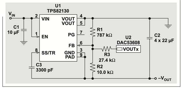
Hello again,
I would like to revisit this topic. In the end for the first iteration of my design I had to go with the LT8643S, as I did not find any way to properly control the output voltage of the LM61460 via a PWM. The FB pin should not be used for that matter according to other posts and in any case in a negative buck setup it would increase highly the design complexity. In the LT8643S I can adjust the output voltage thanks to the TR/SS pin via a PWM. I would like however, if possible, to move to a TI IC, as the LT parts are very expensive. Is there any equivalent solution to the LT8643S in TI which allows a positive or negative output buck design with PWM controlled output voltage?
Thanks,
Javier