This thread has been locked.

If you have a related question, please click the "Ask a related question" button in the top right corner. The newly created question will be automatically linked to this question.

TPS61088: Noise and Compensation Loop Issues

Part Number: TPS61088

Tool/software:

Hello,

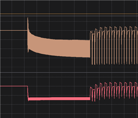
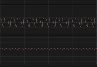
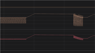
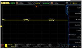
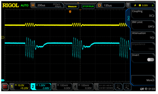
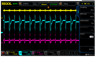
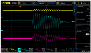
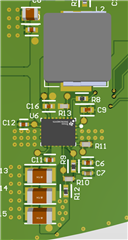
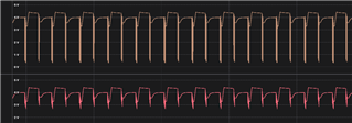
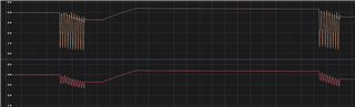
I have attached my schematic and screenshots of my layout along with the scope output.  The schematic isn't entirely correct though.  I have added a 470-uF aluminum cap to the output.  I also add a 47uF capacitor on the input.  R9 is now 15kOhm, C7 is 1nF and C6 is 100pF.  I know R10 and R12 are swapped and have been corrected.  The top signal is the switching signal.  The bottom signal is the power input.  I zoomed in so you can see the ringing.  I also have tried PFM and PWM modes.  


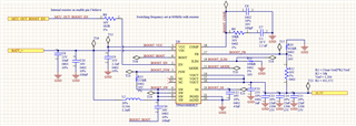
I can make the noise go away if I load it up with a 120ohm resistor to force a load on it.  That makes it run better but isn't the real application.  This needs to turn on for the amplifier IC to actually work so it would be in low load conditions to start with with the noise on the power, the amplifier doesn't work correctly (brownout and gets lost).  So from a practical point, I can't just load this and take it away when I need the normal amplifier functionality.  I also not on my power supply that if I supply the 4V input, I get up to 1 A of power draw for just those resistors.  So with all that being said, how can I get this noise out of the boost regulator without having to load it like this and get it to work as required?  Is it a loop compensation issue?  Is it a capacitance or feedback issue?  Any help is appreciated.  


  • One more note.  Zooming out, I can see that the switcher appears to start normally but then gets to the noise state of things.  So stable power, switching starts and the power drops down to 2.5V from 4V and then it switches to the noisey region.  

  • Hi Greg,

    Not sure the load current when you are making the test, but looks like the COMP parameters are not suitable.

    Considering there is a very large aluminum cap 470uF at output, the R9 C7 should be larger (especially for C7), please refer to section 8.2.2.8 Loop Stability in datasheet for the correct design of COMP parameters.

    Let me know if you have any question.

    Regards,

    Nathan

  • I removed the capacitors and still have the issue where it starts normal then gets the noise again. What are my options? Add the caps back and update the compensation loop or what else do you recommend?

  • Hi Greg,

    Could you confirm the load current during the test? 

    And looks like the output voltage is 10.5V but the top signal, SW (switching signal) high level is not as high as 10.5V, only 4.5V, this doesn't make sense for a normal Boost device, could you please confirm the test point of this waveform? I am thinking if the boost doesn't start-up successfully (maybe due to the larging current during startup? May I know the startup load current of Boost?) so that the output voltage is not 10.5V.

    Also please double check the COMP parameters (R9 C7 C6) matched the design formula in section 8.2.2.8 Loop Stability in datasheet.

    Regards,

    Nathan

  • Hello Nathan,

    Sorry this was a bit confusing.  My load is two 470ohm resistors in parallel.  

    Here are some new scopes. 

    This one is just the output


    This one is the output and the input

    This one is the output, input, and the switching signal.  


    Here is one with the output, input, and another regulator output (1.5V LDO from the same input).

    Each probe added more noise so we take some of this was a grain of salt.  Number 2 looks like what I was seeing.  This is just using a bench power supply.  I have also tried 4X resistors in parallel for more.  I have checked the compensation values and think they should be fine.  

  • Hi Greg,

    Thanks for the sharing.

    We notice that the input capacitor is only 10uF, I suppose there is a long wire when making the test between the power supply and TPS61088, when a ceramic capacitor is used at the input and the power is being supplied through long wires, this may induce ringing at the VIN pin. This ringing can couple to the output and be mistaken as loop instability. In this circumstance, place additional bulk capacitance (tantalum or aluminum electrolytic capacitor) between ceramic input capacitor and the power source to reduce ringing that can occur between the inductance of the power source leads and ceramic input capacitor.

    Considering in the real application, the input source is a battery and I guess no long wire between battery and TPS61088, so the bulk cap is not needed in real user case, but for test case, it would be better to add a bulk cap. Could you try again with the recommend setup? Thanks

    Regards,

    Nathan