Tool/software:
Hi team,
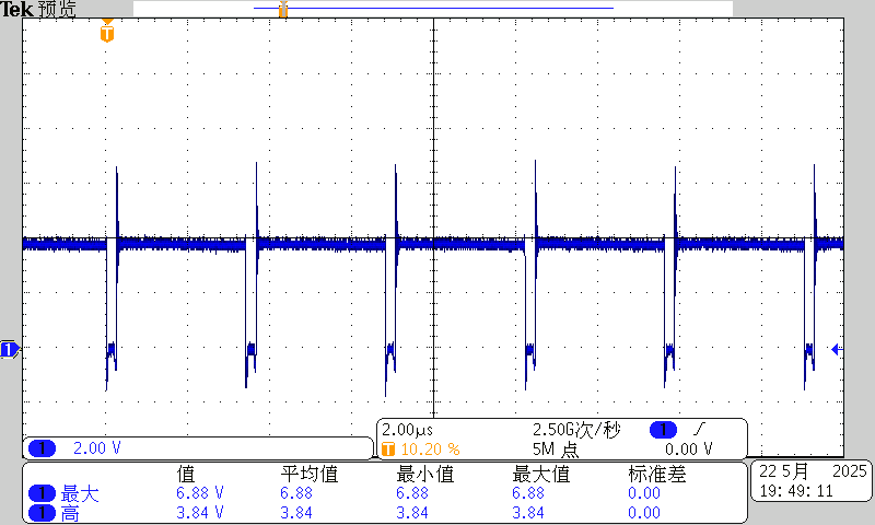
I am an analog FAE in auto Tier1 team. Here is a question about bootstrap of EVM board: Vin pin =12V, Vout=4.94V, f=2.2MHz, the calculated duty cycle should be 4.94/12/2.2=187ns. It is right when I tested the Vds of upper MOS and lower MOSFET. However, when I test the HB-SW waveform (a 0.1uF capacitor in series with a 4.7R resistor, the resistor is additionally added for decreasing SW ring), I found that the discharge time of HB-SW is near 220ns, which is not consistent with the calculated one.
1) In the waveform, which part should be the real discharge/charge time?
2) I know there will be dead time, during which the body diode of lower MOS is in charge of providing current path. This may can explain the uprush voltage after a relatively gentle HB-SW rise? How long should the uprush time be? It seems to more than 10ns.
3) Why there is a sudden voltage drop after capacity discharge?
Thanks a lot. I am a newcome FAE. This question has bothered me for several days, and your response really matters to me. Thanks a lot.
Best regards,
Siv Ma
Following are the waveforms in sequence: 1) HB-SW 2) Vds of upper MOS 3) Vds of lower MOS