This thread has been locked.

If you have a related question, please click the "Ask a related question" button in the top right corner. The newly created question will be automatically linked to this question.

TPS54394: I have an issue about the layout in the datasheet.

Part Number: TPS54394


Tool/software:

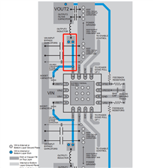
Hi,i have an issue about the layout in the datasheet at 16-17 page,the SW pin of the ic connect to the inductance, that isn't in top layer,but in inner layer,why do it? I observed other DC-DC chips where the SW pins and inductor wiring are on the same layer,so I'm confused.

  • Hi,

    This way analog and non-switching components are away from switching components (physically away on the same layer with electrical connection on bottom or inner layer). Another aspect I can think about is to minimize RE. 

    I observed other DC-DC chips where the SW pins and inductor wiring are on the same layer,so I'm confused.

    You can very well have this implementation too and depends on your application and compliance requirement. This is a very old device and the recommendation for the same might hold true then - I'm not aware about the history but let's follow what has been documented. 

    Regards,

    Gautam

  • HI,thank you for your reply,so but won't drilling holes in this way introduce more parasitic parameters?

  • Depends on the benefits this gives you if compared to introducing parasitics. You can decide for your system.