


Tool/software:
Hello,
I have a few questions:
①Is the VEN pin an open-drain output?
The datasheet states "Open-drain I/O pins (SDA, SCL, HDQ, VEN)".
②The recommended value for the current sense resistor is 5mΩ to 20mΩ, but can I exceed this value?
For a load current of about 0.1A, can I reset the resistance value beyond the recommended value so that the current sense input potential difference is within ±125mV?
For example, a resistance value of 0.5Ω.
I understand that even if a peak current occurs, the potential difference must be kept below ±300mV.
③If the temperature reference is the internal thermistor of the BQ34Z100-R2 instead of an external thermistor, is it okay to float the TS pin since it has a built-in pull-down resistor?
④If two PchFETs are connected in a common source configuration on the BAT+ side for reverse connection protection, will this IC be damaged if the battery polarity is incorrect?
On the BAT+ side, two PchFETs are connected in a common source configuration for reverse connection protection, the battery voltage is stepped down, and DC3.3V is supplied to the REGIN pin.
The voltage to the BAT pin is also connected to a voltage divider resistor circuit, with the battery voltage passing through a reverse connection protection circuit.
Is this a problem?
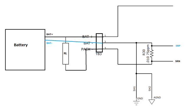
⑥Is it correct to understand the connections of SRN and SRP to PACK- and BAT- as shown in the image below?
RL is the load.
Thanks.

