Other Parts Discussed in Thread: TPS54KC23
Tool/software:
Let's take a look at the application schematic:
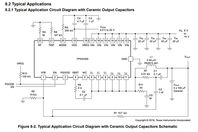
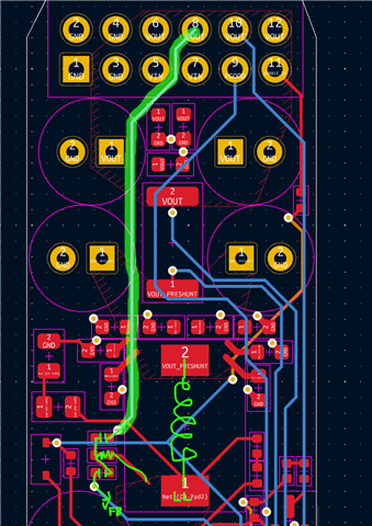
Specifically, let me call your attention to C1, C2, R7. These components are referred to as the ripple injector, and are recommended in the datasheet if you have low ESR MLCCs on the output. I have placed these components, and am getting relatively good control loop stability up to 20A, but I am seeing more ripple than I'd like at the output (about 100 mV pp on this 1.2V rail), and I can't help but think that C1 is partially to blame. R7 and C1 together form a path with impedance 3kΩ + 10MΩ/jω from LL directly to VOUT, which seems ill-advised, and I assume is partially responsible (although I haven't tried desoldering C1 yet, as I don't have very many boards to spare).
Can you folks chime in on the purpose of C1 specifically? I understand how R7 and C2 together increase the ripple on VFB, but I'm not understanding the purpose of C1. Is C1 just about transient response, and giving a faster path from VOUT back into VFB? If so, can I omit C1 if I'd like to trade off worse transient response for less ripple and more control loop stability?
Overall, I should say that while the TPS53355 seems to be pretty good, I have found its control loop to be more sensitive than I would like, ideally. I am driving some sensitive digital FPGA rails, and need very low ripple. Can you folks recommend any other TI parts I could look at that can go down to 0.85V, do at least 30A, and have rock-solid "idiot proofed" control loops? I would much rather give up some transient response to get a rail that never goes down.
Thanks,
-Peter