This thread has been locked.

If you have a related question, please click the "Ask a related question" button in the top right corner. The newly created question will be automatically linked to this question.

TPS1HTC30-Q1: Strange part behavior with no load attached

Part Number: TPS1HTC30-Q1

Tool/software:

Hello,

I am bringing up a design with a dozen TPS1HTC30-Q1s as high-side load switches.  The parts are exhibiting behavior that doesn't match the datasheet and I'm hoping for some input on what might be going on.

All the instances on my board behave the same way, so it's not an issue of one damaged part.  The PCBA is also straight from the assembler and has only been handled in an ESD-safe environment.  I also confirmed the pinout was correct, the part markings match the datasheet, component orientation is correct, and there are no short circuits.

My test configuration is as follows:

  • 28 V supply
  • EN pulled low by microcontroller via 10k series resistor
  • 24.9k on ILIM pin (for a 4 A setpoint)
  • 768R on SNS pin
  • LATCH tied to GND
  • DIAG_EN tied to 3.3 V
  • 100k pull-up on nFAULT
  • No load attached (to start with)

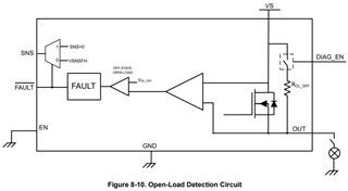
When I first powered up the PCBA, I noticed with a thermal camera that all the TPS parts were heating up by about 10ºC above ambient.  When investigating further, I measured that the VOUT pins were 330 mV HIGHER (!!!) than my supply voltage.  nFAULT was pulled low, consistent with open-load detection, but the SNS pin read 3.47 V, which indicates a roughly 6 A current sense reading. (Again there is no load present, and the total current into the board is much less than 1 A.). That SNS voltage also should not be possible since the datasheet indicates it will not exceed DIAG_EN voltage of 3.3 V.

When I connect a 22R load resistor to the output, the part appears to behave normally.  The heating stops, and the current draw from my 28 V supply drops by about 7 mA.  SNS pin now reads 0, and nFAULT is deasserted.

My design has no boost converters or charge pumps besides the ones in the TPS1HTC30s for the internal gate drivers.  My hypothesis is that somehow the charge pump output is making its way to the VOUT pins and passing through the body diode of the internal MOSFET, but based on the simple internal block diagram and all the information available in the datasheet that really shouldn't be possible.

I will continue investigating - including seeing what happens when I assert EN high (need to make some firmware changes before I can do that) - but wanted to put this out there now in case anyone has seen anything similar.

Thanks!

  • Hi Leo,

    For off-state open-load detection - fault goes low and the SNS pin will read VSNSFH so ~3.3V would make sense here. Can you please completely turn off the TPS1HTC30-Q1 device or remove it and measure the input/output pin voltage to see if something else in the system is causing an offset? A slight voltage offset could also possibly be due to leakage from diagnostics. If you turn DIAG_EN and EN are off, you should see 0V on the output. Can you please confirm this and also that there is not a general offset due to the measuring equipment being used? Do you have any waveforms that we can take a look at?

    Also, we typically recommend 10k for the fault pull-up resistor.

    Best Regards,

    Rishika Patel 

  • Hi Rishika,

    Thanks for your reply.  I agree that a non-zero voltage at VOUT is expected with DIAG_EN high due to the open-load detection, however that should never be higher than the VS voltage based on the block diagram.  Nothing else in my circuit touches that output net, and there are no voltages higher than VS elsewhere in my design either, which strongly suggests the IC is misbehaving somehow, most likely something to do with the charge pump for the gate driver.

    I will need to rework the PCB and lift a pin to disable DIAG_EN, so I haven't tried that yet, but it's on my list.

    I did additional testing today connecting different resistances across the output to see where the behavior changed.  The relevant values are below.  The current draw is for my whole board, so only the changes in that value are relevant.  VS voltage was 27.98 V for all the cases below.

    VOUT load VOUT nFAULT PCB draw SNS Heating observed
    Open circuit 28.322 V 0 186 mA 3.462 V Yes
    1 Meg 26.285 V 0 186 mA 3.462 V Yes
    470k 22.972 V 1 179 mA 0 mV No
    680k 24.659 V 1 179 mA 0 mV No
    820k 25.424 V 1 186 mA 0 mV Yes

    With the 820k resistor however, when I touched both leads at once, reducing resistance via my hands, the heating stopped, current draw decreased by 7 mA, and stayed that way even after I released the terminals.  No change in SNS or nFAULT.  It went back to the fault condition with heating when I disconnected the resistor.

    It looks like there are potentially two separate issues going on here.  The high voltage on SNS does not directly correlate with the increased current draw and IC heating, or with the state of nFAULT.

    I captured the voltages during startup at VS and VOUT with various loads as well.  Green trace is VS, blue trace is VOUT.

    With 22Ω load:

    With 100k load:

    With no load:

    The first two waveforms look as expected given DIAG_EN being high and turning on the internal pull-up for open circuit detect.  In the no load waveform, something odd clearly happens during turn-on, and the voltage ends up settling at the VS + ~340 mV value and holding steady there.  Whatever is going on though isn't purely related to startup conditions, as I was able to produce faulty and normal behavior simply by changing the load connected, I did not turn the power supply off between measurements in my earlier table.

    I can work around the issue by adding 100k in parallel with the load output for each channel, though I lose open circuit detection which is OK for now, but would still definitely like to get to the bottom of this.

    Thanks,
    --Leo

  • Hi Leo,

    Sorry for the delay, I will follow up on this tomorrow.

    Best Regards,

    Rishika Patel 

  • Hi Rishika,

    I conducted some additional testing this morning, using the MCU on my board to toggle the EN pin to the IC.  Here's what I found:

    Initial test with no load connected: 

    • Powered up the board, VS = 27.981 V as before.  VOUT = 28.301 V, same as before.  IC observed to heat up with thermal camera.  DIAG_EN still tied high (needs rework to change).  VSNS = 3.463 also as before.
    • Set EN = 1.  VOUT = 27.981 V (as expected - the FET is on).  Current draw into PCB drops by 7 mA, IC no longer heating.  VSNS = 0 mV.
    • Set EN = 0.  VOUT = 27.815 V (different than before).  Current draw increases by 7 mA and IC is heating up again.  VSNS = 3.463 V again.
    • Repeated the cycle a few times and the behavior stayed the same.

    Whatever is going on here, enabling the device even with no load connected at least stops the VOUT from going higher than VS when it is commanded off again, but the issues of the IC heating up and too high a voltage being present on VSNS both persist.

    For the next test I connected a 120k resistor across the outputs.

    • Powered up the board, VOUT = 12.688 V (roughly where expected since DIAG_EN is on), no IC heating observed, VSNS = 0 mV.
    • Set EN = 1.  VOUT = 27.981 V (as expected), no IC heating, VSNS = 0 mV.
    • Set EN = 0.  VOUT = 12.688 V again, no heating, VSNS = 0 mV.

    These tests confirm that at least the power switch function is working properly, but the faulty behavior with no load attached continues as before.

    Thanks,
    --Leo

  • Hi Leo,

    Yes, you are correct that the input voltage potential should be higher than the output voltage potential. In your case, since the opposite is occurring, reverse current may be causing the device to heat up. 

    It seems even when EN is low and there is a high impedance load connected, there is significant voltage on the output (second waveform and last test). 

    Can you please remove the device and measure the voltage at the input/output nodes? Parasitic effects from the board could possibly cause this voltage offset. Have you tried to replicate this issue on our EVM? 

    Can you please provide a schematic? 

    Best Regards,

    Rishika Patel 

  • Hi Rishika,

    I'll remove one of the ICs and make some measurements to see if any parasitic effects are in play, but I won't be able to get to that for a few days.  I'll follow up when I have more information, likely early next week.

    I have not tried to replicate the issue with the EVM, but I have closely compared my schematic and layout to that reference design and did not see any notable differences.  I'll share a schematic when I follow up after removing the IC.

    Thank you,
    --Leo

  • Hi Leo,

    Thank you, I will wait for your response.

    Best Regards,

    Rishika Patel 

  • Hi Rishika,

    I did some additional testing today after reworking the board.

    On one channel, I lifted the DIAG_EN pin, which was tied directly to +3.3 V on my board.  With that pin floating, the IC no longer heats up, and the voltage at the output is 0 V.

    On a second channel, I removed the catch diode and TVS on the output net.  This did not change any behavior, the output was still 28.315 V.

    On a third channel, I removed the TPS1HTC30-Q1 IC entirely, but left the TVS and catch diode in place.  The output measured 0 V.

    To me this strongly indicates the IC itself is at fault and not the PCB around it.  Can you please loop in someone from the silicon team for this part to see if they have any ideas?

    Please see the relevant portion of my schematic below.

    Thank you,
    --Leo

  • Hi Leo,

    Thanks for your response!

    Let me discuss this with the team and get back to you.

    Best Regards,

    Rishika Patel 

  • Hi Leo,

    The schematic looks fine. 

    We have tested this on our EVM and did not see any issue. If the device is off, there is no path from VS to VOUT besides through the pull up resistor for open-load detection when diagnostics is enabled. The resistor pulls the output to about the same voltage as VS (very slight drop due to the resistor). There should be no possible way for the output voltage to be higher than the supply. 

    Can you please test on an EVM?

    Best Regards,

    Rishika Patel 

  • Hi Rishika,

    Thank you for confirming my schematic looks OK and for trying to reproduce the issue.

    Whatever led to the current state of these parts on my boards, it's pretty concerning in terms of continuing to use this part in this or other designs moving forward, especially since we have no leads yet as to what is really going on here.  Thinking about what the causes could be at a high level: 

    • The issue could be a result of my circuit implementation, however you've confirmed the schematic looks OK, and I followed the layout recommendations in the datasheet and we are well within the specified component ratings.
    • It could be a bad lot of ICs, though that would also be highly concerning given this is an AEC-qualified component. 
    • It could be an issue from the assembly process, though these boards were professionally assembled and we have had no issues with other circuits in the design or any indications of ESD damage, etc., so I don't think this is likely.

    Would you be willing to send me an EVM and a few spare ICs to continue testing?

    Thank you,
    --Leo

  • Hi Leo,

    Please contact the product marketing manager at r-anam1@ti.com to inquire about samples.

    Best Regards,

    Rishika Patel 

  • Hi Rishika,

    Thank you, I will reach out about samples.  In the meantime, if you are able to get any input from the silicon team behind this part I would greatly appreciate it.

    --Leo

  • Hi Rishika,

    I now have the TPS1HTC30-Q1 EVM, and I was able to reproduce the issue.

    My test setup was as follows:

    • No load attached to VOUT
    • Used jumpers on the EVM to set R_ILIM = 24.9k, same as in my design.
    • Adjusted pot on EVM to set R_SNS to 768R, same as in my design.
    • Set EN = 0
    • Set DIAG_EN = 1
    • Set LATCH = 0
    • Connected VIN/GND on the EVM to my power supply, input measured 27.994 V.
    • Measured VOUT to GND at 28.351 V.

    As before, if I set DIAG_EN = 0, the voltage drops to nearly 0 (measured 78 mV).  If I set EN = 1 the internal FET turns on and I see 27.994 V at the output regardless of DIAG_EN state.  Just in case I also tried removing the jumpers for R_SNS and FAULT, which did not impact behavior.

    This was the very first test I ran with the brand-new EVM, no modifications to the board besides jumper settings.

    When you tested with your EVM were you running at 28 V?

    Thank you,
    --Leo

  • Hi Leo,

    I will follow your steps at VS = 28V to see if I can replicate the issue. I had not seen this previously, but I will try again and get back to you.

    Thanks,

    Rishika Patel 

  • Hi Rishika,

    Quick follow-up, I'm also observing the issue at lower voltages - 12.0 V input produces 12.365 V output.

    Thanks,
    --Leo

  • Hi Rishika,

    Following up about this issue again, do you or your team have any insights?

    Thanks,
    --Leo

  • Hi Leo,

    So sorry for the delayed response, I was out of office last week. 

    I apologize, I am seeing something similar to you this time. I measured the voltage on the input and output pins during open load on the EVM and the output was ~0.3V higher than the input. The heating may be due to the fact that VS is being dropped over the internal open-load pull up resistor and it is a fault condition for the device. It does not seem to be an issue as 0.3V should be less than VF of the body diode of the FET so it is technically not conducting in the reverse direction.

    I am following up with the design and systems teams so I will update once I have more information.

    Thanks,

    Rishika Patel 

  • Hi Leo,

    I apologize for the delay. I was able to discuss this with the design team. The reason for what we are seeing is that there is some circuitry between the charge pump and the VOUT rail which is enabled due to DIAG_EN being high. So, there is some IQ being dumped on the output pin. Some of the blocks are sourcing more than sinking which is why the output voltage potential is slightly higher than the input. Again, this should not be an issue with normal operation of device.

    Sorry for the confusion and I hope this helps provide more clarity on your observations. Thank you for your patience!

    Best Regards,

    Rishika Patel 

  • Hi Rishika,

    Thanks for the additional information.  The issue with this component in my design is less that the output voltage is a little high with no load, though that is an interesting symptom.  My problem is the power dissipation from the IC when in this condition.  From my measurements the IC draws an extra ~7 mA when experiencing this condition, or nearly 200 mW of additional power dissipation (for a 28 V supply).  Especially when you have multiple channels in a design, that adds up quickly.

    If this is a known issue or limitation of the device, it really needs to be captured in the datasheet.  Looking at the Electrical Characteristics table, quiescent current is not specified for the state where V_EN = LO and V_DIAG_EN = HI, which is when we see the faulty behavior.  The quiescent current spec given for when V_EN = HI suggests a difference of 100-400 uA depending if V_DIAG_EN is LO or HI, which seems perfectly reasonable given how the feature is implemented.  The Functional Block Diagram also gives no indication that off-state open load detection involves anything other than a simple pull-up resistor and transistor switch.  Are you saying that off-state open load detection is not considered a normal operating mode of the device despite being a key feature in the product description?

    Had this phenomenon been conveyed in the datasheet, I would have provided a means to toggle DIAG_EN in my design, perhaps even individually per channel given that some are intended as spares, or would have selected a different part entirely.  The specs that were provided suggested a difference of only a few hundred uA to leave DIAG_EN enabled all the time, so having that turn out to be 20-70x higher seems like a pretty major omission.

    Thanks,
    --Leo

  • Hi Leo,

    Open-load fault reporting is part of the diagnostics features. An off-state open load condition is a fault state which is reported on the SNS and fault pins. In the on-state, the user has to observe if there is an open-load condition and it will not be reported.

    Leakage is measured on the VS to VOUT path when EN is off; there is going to be some leakage present due to the internal logic control path. The leakage by diagnostics is caused when this switch controlled by DIAG_EN is on. This leakage is known and is not faulty behavior as it does not affect device functionality or cause other issues. 

    I measured the current at the ground pin and the highest current I saw was ~2mA when EN is low. I saw ~1mA when EN is high. 

    Thanks,

    Rishika Patel 

  • Hi Rishika,

    I did some additional testing with the EVM and I'm seeing pretty different numbers than you are for ground current.  I connected a bench DMM to the pins of J1 on the EVM to take the measurements, and powered the board with voltages from 12.0 V to 28.0 V in 5 V steps.  No load connected to the output.

    • With EN=1, the ground current was right around 1.12 mA the whole time, increasing slightly from 1.118 mA at 12 V to 1.123 mA at 28 V.  Power supply current into the whole board was 2.9 - 3.1 mA.
    • With EN=0, the ground current was 4.32 - 4.33 mA across the voltage range.  Power supply current however was 10.8 mA.

    After further investigation, I found that if I removed the jumper that connects the SNS pot (J7), the ground current increased significantly, though the total draw from the power supply stayed roughly the same.

    • With EN=1, the ground current was nearly the same as before, around 1.15 mA.
    • With EN=0, the ground current was 8.82 - 8.83 mA across the voltage range, and power supply current was around 10.5 mA.

    So it looks like the IC ground current isn't the whole story here, which makes sense given the relatively low sense resistor values used with this part and that the SNS output voltage "rails high" to just above the DIAG_EN pin voltage when no load is present.  But the part is drawing the current and dissipating extra power either way, regardless which return path ends up carrying it.

    At this point the problem is mostly moot, the behavior of the IC isn't going to change and my PCB design using these ICs is what it is for now.  My point in pressing this issue is that this effect is not documented at all in the datasheet, despite being known to TI as you have indicated, and in some applications that extra ~7-8 mA or so of current draw could be a real design consideration.  In my application (at 28 V) each IC drawing 8.8 mA with EN=0 and DIAG_EN=1 and no load connected is dissipating about 230 mW - as confirmed with a thermal camera - and at the max rated voltage for the part (48 V) it would be nearly 400 mW.  It's simple to work around the behavior by designing to be able to control DIAG_EN, but much harder to implement a fix if you only find out about the behavior once you already have hardware in hand that ties DIAG_EN high...

    Thanks for the help working through this.  I hope to see an updated datasheet in the future that describes this behavior so no one else is taken by surprise.

    --Leo