This thread has been locked.

If you have a related question, please click the "Ask a related question" button in the top right corner. The newly created question will be automatically linked to this question.

TPS7A02: LDO shutdown problem

Part Number: TPS7A02

Tool/software:

Hi,

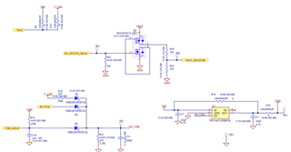
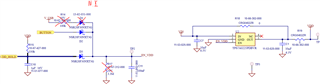
I encountered problems with the TPS7A0225PDBVR on our PCBs. It looks like the EN pin is making the LDO shutting down because when I bypass the LDO, the PCB works fine. Apparently in the datasheet if this pin is in floating state the LDO is shutting down. I'm pretty sure this problem is occuring but I don't understand why. Is this component sensitive to EMC/vibrations problems ?

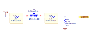
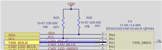
The power on working is simple, first, you push the button S1 and then the MCU sends 1.33V on the VDD_HOLD pin. You can find the schematics for better understanding. 

If you could help me understanding the behaviour of the TPS7A0225PDBVR I would be more than grateful. Thanks

Regards,

Leo

  • Hi Leo,

    To your point on floating EN, VEN must be greater than VEN_HI (1.1V min) for the device to turn on. If VDD_HOLD is 1.33V like you mentioned, note that D2 is forward biased between VDD_HOLD and EN_VDD. The forward voltage drop for this diode would make EN_VDD less than VEN_HI and so the part will not turn on. This is expected behavior with your current circuit setup.

    Please increase VDD_HOLD. You can confirm this by bypassing your current EN mechanism and externally provide a bias at TP2 and check the output of the LDO

    Regards

    Ishaan

  • Hi,

    Thanks for you answer. Sorry I have missed informations. The 1.33V was measured after the diode, on TP2. Our product is working fine, but sometimes it will randomly shut down. And futhermore, I have incorrectly explained the working principle.

    You first press the button so 3V -200mV is sended to EN_VDD, then the LDO is creating the VDD which is 2.5V. The VDD is now passing though R15 and R17 and now there is 1.33V measured on TP2. The product is seld maintened with this principle.

    The VDD_HOLD is only used to shutdown the product where there is a long press on the S1 button.

    Could you also tell me if the implementation is correct ? I know it's not perfect because C1 isn't as close as it is recommended in the datasheet. Thanks

    Regards,

    Leo

  • I know it's not perfect because C1 isn't as close as it is recommended in the datasheet. Thanks

    You are within the recommended range for COUT.

    My concern is with the rest of the implementation. You are generating a voltage rail with the LDO which then powers the enable logic in a way. Any significant change in VBAT can cause the LDO to go into dropout and this will reduce the voltage seen non TP2 and disable the LDO

  • Could you tell me what's the voltage range of the "significant change in VBAT" ? The battery on VBAT is a VARTA CRAA LiMnO2 which goes from 3V to 2V.

  • The lower limit for VBAT would be what puts the LDO in dropout such that VEN is below 1.1V (min). Dropout depends on a lot of factors. Please let me know what your load current is

  • I would say the max current is 80mA for 5s every 1 hour, and between it's 10uA. It's a LoRaWAN product

  • Then the dropout is between 100-150 mV. I noticed you said that VIN can go to 2V. Please note that anything below 2.65V on VIN for a 2.5V output voltage device will put it in dropout.

  • Our product is working fine in dropout mode we have tested to supply it with external power source of 2.2 volts and it's working.

    Something else is triggering me, I don't really understand the true working principle of the Ren pulldown. When I mount a 10k on R15, I measure 2.45V on TP2 (so Ren pulldown disabled as exepected like on the datasheet), but when I mount a 100k on R15, I measure 2.2V on TP2. It looks like the Ren pulldown is supposed to be disconnected, but in reality it's not, and it's creating a voltage divider with 2.5V, 100k and 500k (the value of the Ren pulldown)

  • I will show your schematic to another engineer on our team because I am confused with this implementation as well. We can get on a call too if you are okay with it?

  • Thanks for sharing, I will wait the written answer no problem.

  • I will update here once I have an answer

  • Hi, I'm looking for updates, anything new ?

  • Hi Leo, I dont have an update yet

  • Hi Leo,

    We talked about this and our team had the following questions and requests for you to debug further:

    1. We feel leakage current through D1 and D2 is pulling EN_VDD low when the EN circuit is supplied from VDD and controlled by VDD_HOLD. Schottky's have larger reverse voltage drop under reverse leakage current.
    2. Do we know the current from PA2 of the Microcontroller?
    3. Please do the following to debug: Replace D1 and D2 by standard diodes and retest, Please probe VDD, EN_VDD, and VDD_HOLD

    I will wait for your response