This thread has been locked.

If you have a related question, please click the "Ask a related question" button in the top right corner. The newly created question will be automatically linked to this question.

LM5156-Q1: SEPIC converter - MOSFET overheating

Part Number: LM5156-Q1
Other Parts Discussed in Thread: LM5156

Tool/software:

Hello!

I need some help to troubleshoot this SEPIC converter on my project.

The goal was to design a power supply with the basic specs below:
Vin => 8V ~ 48V, 24V nominal
Vout => 24V
Iload => 3A max

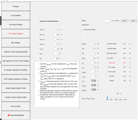
Using both WEBENCH and the spreadsheet SNVR481 we came up with the design below:

/resized-image/__size/320x240/__key/communityserver-discussions-components-files/196/pastedimage1748913144995v2.png


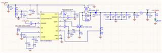
Please note that the value for R86 is wrong. It should be 3.3k instead of 33k. Also, R75 is unmounted.

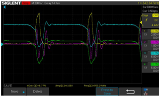
The converter works and regulates under load, although with only 1A, the MOSFET reach up to 100ºC in 5 minutes.

We captured some pictures to try to figure out the issue.

Yellow: Gate Voltage

Purple: Source Voltage

Blue: Drain Voltage

Green: Diode Anode

0A Load:

2A load:

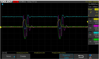
I'm really confused. Since these images were captured with 24V on the input and on the output, I was expecting to see around 50% duty cycle. What could be the cause for this low duty cycle? I checked and the on time is close to the minimal on this switching frequency.

Also, the gate curve does not look good. It looks quite slow. Can it be the reason for the MOSFET dissipating too much power?

  • SEPIC schematic.pdf
    I don't know why, but the schematic photo was uploaded with very low quality. Here's the same image on a PDF

  • Hi Wagner, 

    Thank you for using e2e forum.

    Could you also please attach the filled spreadsheet - SNVR481.Also, please help to send the clear screenshot with the divisions seen clearly of the signals - Vin, Vout, SW node and current sense pin. 

    Best regards,

    Mounika

  • Hi Mounika,

    Thank you for the help.

    The spreadsheet and the pictures you requested are attached. It turns out that the previous pictures were not captured correctly. On the new pictures we can see a duty cycle closer to 50% under load conditions. I'm sorry for that. Although, we still have the overheating problem with the MOSFET. 

    On the pictures with multiple signals:
    Green = Vout;
    Blue = Vin.
    Yellow = MOSFET gate;
    Purple = IC CS pin.

    On the picture with only one signal, the signal is the switching node.

    5810.SEPIC.zip

    4705.LM5155_56_Excel_Quickstart_Calculator_for_SEPIC.xlsx

  • Hi Wagner, 

    Thank you for filling out the QS calculator and sending the clear picture. 

    The waveform looks betternow. However, the CS pin in the 2A load screenshot doesnt look good. I am guessing it is the measurement issue.

    The estimated total losses in the MOSFET is approx 2.5W and it needs to be cooled 

    • Depends on if enough copper is usd in the layout to cool
    • Changing to another FET
    • or switch with lower switching frequency

    You could also download https://www.ti.com/tool/POWERSTAGE-DESIGNER and try it yourself.

    Best regards,

    Mounika

  • Hi Mounika,

    Thank you for the suggestions.

    You are correct. The signal on the 2A screenshot was saturated. I attached a new one.

    2A_corrected.zip

    How can I predict if I will need cooling or not? 2.5W seems low to me considering that the MOSFET datasheet lists 0.63K/W  as the thermal resistance. It doesn't say the cooper area considered for this data. However, in reality it reaches more than 100ºC in just a few minutes. Something seams off to me. FYI the MOSFET is soldered on a 116mm² cooper area only on top layer. I don't know if this is considered too small or not. 


    I tried a lower switching frequency, but it didn't get much better than the original one. My guess is that the main losses are the conducting ones.

    Also, I tried an external VCC, of around 10V, to check if the MOSFET was heating because of a low gate voltage. No big improvements here as well.

    I guess I can try to cool it if there is nothing else clearly wrong on the circuit, but how could I have forseen it? Am I missing something?

  • Hi Wagner,

    I can get back to you in the middle or end of next week because we have limited bandwidth at the moment with vacations on 9.6.2025. Meanwhile, could you please try it with another MOSFET to check. 

    Thank you for your patience.

    Best regards,

    Mounika

  • Hi Wagner, 

    did it help to change the FET?

    Best regards

    Moritz

  • Sorry for the long delay, Moritz.

    It helped indeed. We tried only one other MOSFET we had available. The original one was the BUK7Y7R8-80E and the new one is the BUK7M17-80EX.

    From the datasheet, the only spec on which the new one is better is the gate charge, which is almost half of the original.

    Yet, it performed way better. With an 1A load, the MOSFET temperature droped from 70C to 50C. With 2A, the original one surpassed 110C realy fast, while the new one was stabilizing below 90C.

    That indicates to me that the main issue was regarding the switching losses. Maybe the LM5156 was not being able to drive it properly beacause of the bigger gate charge or there was some severe ringing on the gate causing excessive losses.

    We also tested the efficiency: 

    The losses went from 8.5W to 5.2W. The efficiency seems reasonable for me. What do you think?

    We also tried lowering the switching frequency to aroiund 380kHz, which is less than half of the original one. Although, it didn't change significantly the efficiency. That indicates to me that now we are dealing mainly with conducting losses, right?

    For now we will focus on cooling the MOSFET properly.

  • Hi Wagner,

    I am happy to hear that you found a solution!

    I still think its strange, because of the MOSFET parameters, both FETs should work. Also the driver of the IC is strong enough to drive both FETs properly..

    Regarding the losses in the FET, please use the power stage designer to see how the losses are distributed in different conditions https://www.ti.com/tool/POWERSTAGE-DESIGNER   - First select the topology you use and insert the circuit specs, then choose- FET losses calculator- on the left side:

    You can also easily compare both FETs. 

    Is it possible that there  was a bad solder connection for the first FET and that this was the reason for it to heat up so much? Did you try to resolder it or solder a new FET before changing?

    Best regards

    Moritz