REF200: Question regarding 3-wire RTD sensing with REF200AU/2K5

Part Number: REF200
Other Parts Discussed in Thread: INA326,

Tool/software:

Hi TI Team,

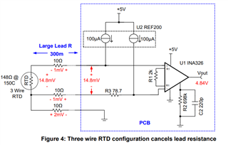
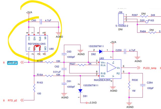
Our end customer is using a 3-wire RTD configuration with your REF200AU/2K5. They have a question regarding the impact of lead wire resistance.

In their setup, they are measuring approximately 0.9 ohms between the compensation lead and one of the RTD signal leads (effectively between what would be Pin 2 and Pin 3 in a typical 3-wire setup connected to an ADC or signal conditioner).

Per their understanding, this 0.9 ohm difference might cause the "noise" cancellation to be less accurate, potentially resulting in actual temperature readings that are lower or higher than the nominal value.

Could you please advise on the following:

  1. For the REF200AU/2K5, what is the acceptable tolerance or matching requirement for the lead resistances in a 3-wire RTD configuration to ensure accurate temperature measurement?
  2. Specifically, would a 0.9 ohm mismatch, as described, significantly impact the accuracy of the temperature reading when using the REF200AU/2K5?
  3. Are there any recommended calibration steps or compensation techniques within the REF200AU/2K5's features or in the accompanying circuitry that can mitigate the effects of such a resistance imbalance?
  4. Could this level of resistance imbalance cause any other issues with the device or the measurement system?

The customer's initial question was: "In the ideal case, pin 2 and 3 are shorted and near 0 Ohm but our test team's measurement, there is a 0.9 Ohm. Could you check if there is 0.9 Ohm across pin 2 and 3, will it cause any issue?"

Any guidance or documentation you can provide on this would be greatly appreciated.

Thanks

  • Hi Hatzrill,

    Thanks for your question!

    Could you please provide a schematic of the customer's design to help me better understand what their system looks like?

    Is the customer implementation similar to this schematic below but with different lead resistance values where it is labeled as 1mV (10Ohm) here? If not, could you please help clarify where the 0.9Ohm difference is being measured?

    In general, a voltage difference between the two inputs to the op-amp (in this example, the INA326) will cause a different Vout value, and this can be calibrated via software.

    Please find a design guide for a 3-wire RTD here: https://www.ti.com/lit/ug/tidu969/tidu969.pdf

    For further support, could you please provide a customer schematic and help clarify where the customer is seeing this resistance difference?

    Best Regards,

    Andrew Li

  • Hi Andrew,

    Sorry for late reply.

    You may refer below of our schematic for your reference. 

    FYI, we measured 0.9 Ohm from pin 2 and 3

    Best Regards

    Hatzrill

  • Hi Hatzrill,

    Thanks for the update!

    It is true that the 0.9Ohm difference may cause an offset in the measured output voltage, but this impact should be small. Additionally, system software can be adjusted to take this into account.

    For further support, could you please provide some characteristics about the customer's RTD? What is the resistance measured at min/max temp, and could you please provide the missing schematic section following nets RTD_p1 and RTD_p2?

    I hope this helps!

    Best Regards,

    Andrew Li

  • Hi Andrew,

    Based on our customer's feedback, the damage at U80 does not related to the resistance max and min temperature because as referring to schematic diagram, RTD sensor is not connected at J60 at customer tools.

    Regards

    Hatzrill

  • Hello Hatzrill,

    Can you please describe the damage being seen at REF200? Also, J60 is not included in the schematic you shared, can you please include that portion of the schematic?

    Thanks,

    Jackson

  • Hello Jackson,

    The failure for the REF200AU/2K5 part is an observed 0.9 Ohm resistance between pins 2 and 3. RTD sensor is not connected at J60 when power up at tool and U80 is damaged.

    Please refer below for the schematic diagram for the J60 locations. 


    Regards

    Hatzrill 

  • Hello Hatzrill,

    I do not understand the significance of REF200 having a resistance between pins 2 and 3 since pin 3 of REF200 is unconnected. Is this what you mean?

    Are you seeing changes in the current being sourced in the REF200 after it is damaged? Additionally, can you please describe, provide photos, or provide scope captures to show how REF200 was damaged?

    Thanks,

    Jackson

  • Hello Jackson,

    We load the resistance between pins 1 and 2, not pins 2 and 3 (pins 2 and 3 are GND).
    Referring to end's customer reply:
    Measurement pin 2 and 3 is shorted and near 0 Ohm, but from Plexus test engineer's measurement, there is a 0.9 Ohm.

    Regards

    Hatzrill 

  • Hello Hatzrill,

    It seems like measurement pin 2 and 3 are different from pin 2 and 3 on the REF200. However, I do not see measurement pin 2 and 3 on the schematics you have provided. I see "RTD_p1" and "RTD_p2", which I could maybe assume are pin 1 and pin 2 of the measurement pins, but you have not mentioned pin 1 being a problem, so I assume that isn't what we need to look at here. Additionally, you have not provided any more information regarding what sort of damage you are seeing on the REF200.

    Is the customer implementation similar to this schematic below but with different lead resistance values where it is labeled as 1mV (10Ohm) here? If not, could you please help clarify where the 0.9Ohm difference is being measured?

    If you would like more assistance, please provide a clearly labeled schematic or block diagram as is shown above with the 0.9Ω measurement clearly labeled alongside measurement pins 1, 2, and 3. 

    It is true that the 0.9Ohm difference may cause an offset in the measured output voltage, but this impact should be small. Additionally, system software can be adjusted to take this into account.

    For further support, could you please provide some characteristics about the customer's RTD? What is the resistance measured at min/max temp, and could you please provide the missing schematic section following nets RTD_p1 and RTD_p2?

    Can you also provide a response to what Andrew has asked for above? Why can the 0.9Ω not be accounted for in system software and can you please provide more details about the customer's RTD, including missing schematic sections?

    In summary, for further assistance, please provide all of the following items:

    1. A schematic or block diagram with the 0.9Ω measurement, REF200, and measurement pins 1, 2, and 3 clearly labeled.

    2. A detailed description, photos, or scope captures that outline the damage and/or change of behavior of REF200 that you mentioned previously. 

    Thanks,

    Jackson

  • Hello Jackson,

    The RTD sensor wasn't connected into the J60 connector when the tool was turned on, and the U80 is damaged. The statement also suggests that since there's no load attached, the damage to U80 wasn't caused by the resistance, or the maximum and minimum temperature readings.
    Also, here is the missing schematic for section following nets RTD_p1 and RTD_p2: 
    Regards
    Hatzrill 
  • Hi Hatzrill,

    I am still not sure what you mean when you say there is damage to U80. My previous understanding is that there was a 0.9Ohm resistance measured between pins 2-3 of U80, but this is not relevant as pin 3 of U80 is NC. Could you please provide more information about how the IC is failing?

    If you are measuring 0.9Ohms difference between the rails going into pins 2&3 of the comparator (U83) this can be accounted for in software as stated before.

    It is true that the 0.9Ohm difference may cause an offset in the measured output voltage, but this impact should be small. Additionally, system software can be adjusted to take this into account.

    For further support, please clearly define what damage you are seeing and where it is found. Also, please clearly define the system setup for your tests.

    Best Regards,

    Andrew Li