This thread has been locked.

If you have a related question, please click the "Ask a related question" button in the top right corner. The newly created question will be automatically linked to this question.

TPS23751: Evaluation of TPS23751 for Use in 10G Base Applications

Part Number: TPS23751
Other Parts Discussed in Thread: PMP11254, ,

Tool/software:

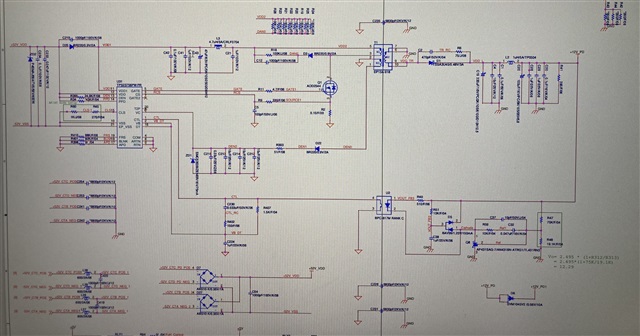
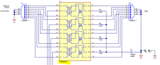
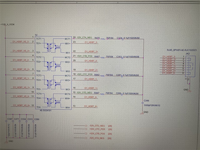
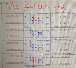
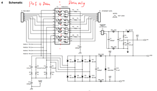
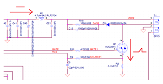
I would like to replicate the TPS23751 circuitry from the PMP11254 reference design and apply it in a 10G Base network environment. However, since the original reference design is intended for a 1G Base network, I would like to ask what additional considerations or potential issues I should be aware of when using it in a 10G Base application?

  • Hi Jacky,

    Thanks for reaching out!

    Sorry that PoE mainly focusing power aspect. The data speed is mainly related to the data transformer. In PMP11254, 749022016 is applied. If it cannot meet the 10G base network please consider a different one with same 25.5W capability. You may check with Ethernet PHY experts.

    Best regards,

    Diang

  • I have already replaced the 749022016 transformer, and the 10G Base network has been successfully verified to work—but only without the PD circuitry connected. Previously, when we added our own PD circuitry, communication errors consistently occurred. Therefore, we are looking for a ready-to-use PD circuit design that has proven experience working reliably with a 10G Base network.

  • Hi Jacky, 

    Can you share the schematic and the data transformer datasheet? It may be the pins connection issue. One common miss is the CM choke of the data transformer is usually on the data only side, rather than the PoE + data side.

    Bes regards,

    Diang

  • The transformer specifications and circuit are as follows

  • Hi Jacky,

    Thanks for the documents. 

    The transformer you shared is the flyback transformer. The data rate is related to the data transformer which is near the RJ45 port like below. Could you share that one?

    Best regards,

    Diang

  • The datasheet and circuit of the data transformer are as follows.

    Datasheet : www.appselectronics.com/.../download.php

  • Hi Jacky,

    It could be the issue I mentioned. Please check the side of PoE+Data and Data only could be revised

    One common miss is the CM choke of the data transformer is usually on the data only side, rather than the PoE + data side.

    Best regards,

    Diang

  • The left side of the transformer is the PHY, and the right side is the RJ45. Since the PoE power always comes from the RJ45 side, the PD must be connected on the right side. If it's connected on the left side, the DC power from PoE would be isolated by the transformer, so there's no way for any power to be delivered.

  • Hi Jacky,

    Thanks for your reply.

    In most of cases (90% or higher), the data transformer on PoE side is without CM choke as below diagram of TPS23751EVM-104 EVM. I would recommend you to double check with your data transformer vendor. If it is wrong, you may consider reversing the data transformer to make your CM impedance of data side or maybe data speed won't be influenced.  

    Best regards,

    Diang 

  • We previously tried reversing the transformer, but it didn’t help.

  • Hi Jacky, 

    Thanks for your information. If the data transformer does not cause the issue, you can check the layout of the RJ45 termination and PD input circuits. Check list is shown below.

    Besides, have you saw the data issue is related to the power load? Will the behavior the same with 0% and 100% load?  

    I have already replaced the 749022016 transformer, and the 10G Base network has been successfully verified to work—but only without the PD circuitry connected. Previously, when we added our own PD circuitry, communication errors consistently occurred.

    Input Section      
    Ground Layers Primary At least one layer dedicated to ground, respecitvely. Any unused space in a layer should be filled with ground plane. Multiple ground layers / planes should be stiched together with vias. Ensure each of the listed ground planes do not overlap: for example the secondary ground on the top layer should not cross over to the primary ground space on the bottom layer.  The chassis GND, VSS_PSE, PGND and GND_D do not overlap
    Secondary
    VSS
    Bob-Smith/ Earth Ground (optional)
    Input Related Components PHY congregate towards RJ-45 input connectors. Treat the BS plane as a phantom or literal earth connection and use it to create a top and bottom layer. These traces should not be oversized -- try to keep the connections short
    ground plane that surrounds the input-related circuitry. Maintain a 0.060” high voltage spacing between
    the BS plane and all other circuitry.
    The distance between BS plane and other circuitry is < 0.06"
    Bob-Smith terminations
    filtering components
    Input Rectifier Bridge   Keep as tight as possible. Keep planes to a minimum by using close spacing. However, this section includes the power path, so the power path needs planes and the passive components can use small traces The power path uses plane and passive components are connected using wide short traces
    Input EMI Filter ferrite beads Ensure there is no copper underneath the common mode chocke or the ferrite beads.  Common mode choke in on L1, ferrite beads are on L12. No copper underneath ferrite beads or common mode coke
    EMI choke
    capacitors

    Best,

    Diang

  • I have confirmed that the issue occurs under heavy load, but I'm not sure what specific effects are actually being caused by the heavy load.

  • Hi Jacky, 

    Thanks for your reply. It could be the TPS23751 generated EMI. Have you tested the EMI of the board? The CM choke in the data transformer will be worse too if its on the PoE side since the CM current is higher and more easier to saturate the chokes. 

    Best regards,

    Diang

  • To prevent saturation, should we change the inductance value or detect the current?

  • Hi Jacky, 

    CM choke could saturate when its CM current is beyond the rating. Since PoE current is CM current in the wire, when the load increases the CM choke could be over its rating.

    Best regards,

    Diang

  • So it's the CM choke that's saturating? How can we confirm that?

  • Hi Jacky,

    You need to reach out to the data transformer vendor. Assuming your PD is 2-pairs, 25.5W Pin and 42.5V.  Make sure each of your CM choke inside the data transformer won't saturate at 25.5W/42.5V = 0.6A.

    Best regards,

    Diang

  • Should the current be based on the average or the peak (instantaneous) value?

  • Hi Jacky,

    The switching loss is with the peak current and the conduction loss with the rms current for hard switching flyback. For class-4, this FET is normally 150V, 50m - 150mOhm rated, normally ~80mOhm for optimizing. 

    Best regards,

    Diang 

  • We will close this issue for now and proceed with a new PCB revision to verify again.