This thread has been locked.

If you have a related question, please click the "Ask a related question" button in the top right corner. The newly created question will be automatically linked to this question.

TPS7B86-Q1: TPS7B8601BQDDARQ1

Part Number: TPS7B86-Q1

Tool/software:

Hello Team,

In our design we are going to use TPS7B8601BQDDARQ1 IC for which we have created the design, Can you please review it.

Vin : 5V to 20V

Current Consumption : 0.4A

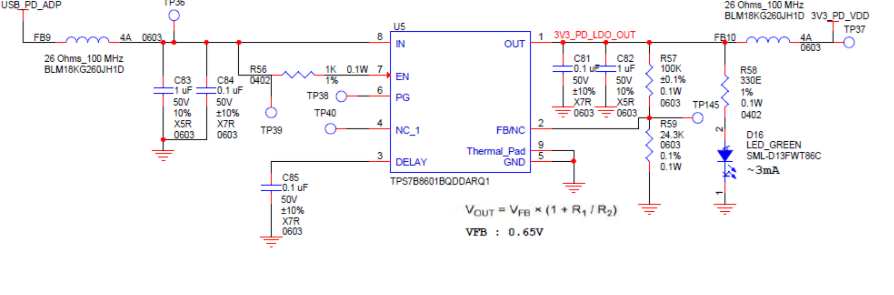
What would be the Power dissipation from this IC ?

Regards,

Tirthal Patel

  • Hello Tirthal,

    * The TPS7B8601BQDDARQ1 does require an output capacitor with ESR > 1mΩ and a capacitance larger than 2.2 uF as depicted in figure 6-39 from the datasheet.

    We recommend selecting a larger capacitor that meets the ESR characteristics.

    * If the input supply is more than a few inches from the regulator, an electrolytic capacitor with a value of 22 µF and a ceramic bypass capacitor are recommended at the input.

    * If the operating ambient temperature is 85C, the maximum power dissipation across the pass element is 1.55 watts. At 400mA and 3.3v at the output, the maximum recommended input voltage is 7.1 V. 

    Best regards,

    Daniel E.

  • Hell Daniel,

    I have updated the design file please have a look : 

    PD LDO.xlsx

    I have also attached BOM for the components used in the design !

    As per the datasheet it mentions that Vin supports ,3 V to 40 V (42 V max) ,So can you please clarify why it mentions "maximum recommended input voltage is 7.1 V."  ??

    Regards,

    Tirthal Patel

  • Hello Tirthal,

    Please make sure the input and output capacitors are as close as possible to the input and output pins. I suggest a 2.2 uF input capacitor to compensate for the DC bias derating.

    I suggest adding a 5-milliohm resistor in series with the output capacitor to make sure the ESR requirement is met.

    I calculated the maximum power across the pass element assuming a maximum operating ambient temperature (the air temperature around the regulator) at 85 ºC

    TA + RθJA * PD ≤150 ºC   →   85 + 41.8 * PD ≤150 ºC   →   PD = 1.55 watts.

    P= ILoad * Vdrop 

    Vdrop = (Vin - Vout), ILoad = 0.4 A

    P= 0.4 A * (Vin - Vout)

    Vin = (1.55 w / 0.4A) + 3.3v

    Vin = 7.1v

    If the junction temperature exceeds 175C, the device will turn off and will restart once the internal temperature is close to 150C. This could create a thermal cycling event where the regulator will turn on and off intermittently if the heat is not properly dissipated. Please note that this calculation is based on JEDEC standard high K profile,JESD 51-7. Please consult section - 6.4 Thermal Information - in the datasheet for details.

    You can add a buck converter at the input and reduce the voltage to 5 v and use an LDO to increase the efficiency of your circuit.

    Best regards,

    Daniel E.