Other Parts Discussed in Thread: CSD17308Q3
Tool/software:
Hello,
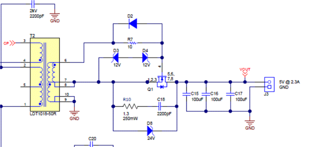
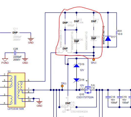
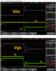
Revisiting another aspect of my TPS23758 design and the EVK design. I'm probing Vgs and Vds to ensure they are in spec for the output FET. While comparing my original faulty design with the EVK and my new proposed design, I found something questionable with Vgs appearing to be out of spec:
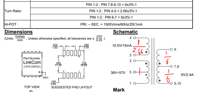
| Design | Vgs | Vds | Vds Snubber | SRF | MOSFET | Vgs rating | Vds rating |
| Original Faulty | -28.8V peak | 35V peak | none | 10 ohm | TI CSD17308Q3 | +/-20 | 30V |
| EVK | -26V peak | 29V peak | 1.3ohm/2.2nF | 100 ohm | TI CSD17579Q3 | +10/-8 | 30V |
| Proposed New | -25V peak | 22.2V peak | 1.3ohm/10nF | 50 ohm | TI CSD18543Q3 | +/-20 | 60V |
The recommended 30V MOSFET has a Vgs limit of +/-20V and it appears like the inductive spike at switching edges of Vgs are out of spec for the parts, despite the steady state voltage being 14V or so. I consider my original design faulty because the MOSFET would fail over time, I don't know if it was due to Vgs or Vds being out of spec, but I would ideally like both voltages to be in spec.
Note, all designs have the appropriate back to back 12V zeners for Vgs clamping.
My questions are:
- Is this Vgs voltage expected for the design? (seems like it is, given the EVK has this)
- Are the two +/-20V TI FETs ok with this over voltage on Vgs?
- Could a snubber circuit be added to Vgs to address this?
These are the scope traces of Vgs and Vds on the TPS23758 EVK design for reference.
Thanks!
Matt