This thread has been locked.

If you have a related question, please click the "Ask a related question" button in the top right corner. The newly created question will be automatically linked to this question.

TPS4811-Q1: while TPS48111-Q1 works alone without MCU, can user send the INP_G and INP pulling up signal asynchronously

Part Number: TPS4811-Q1
Other Parts Discussed in Thread: CD40194B

Tool/software:

Dear team,

My customers want to use TPS48111-Q1 without MCU control.

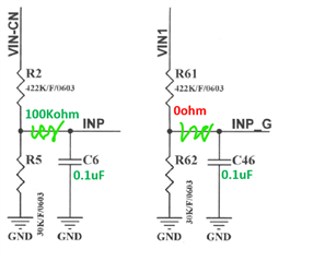
they tied the EN/UVLO and INPG/ INP to the VS pin 48V over resistor dividers. in this case, the INP and INP_G were pulled up almost synchronously.

now their control sequence want to pull up the INP_G first and then the INP to decrease the inrush current.

how does BU site recommend for the this non-MCU based additional circuit?

is cd40194b suitable here?

https://www.ti.com/lit/ds/symlink/cd40194b.pdf?ts=1749124449060&ref_url=https%253A%252F%252Fwww.ti.com%252Fproduct%252Fzh-tw%252FCD40194B

Best regards,

Hank Lin

  • Hank,

    The CD40194B is a bi-directional shift register that has "NO RECOMMENDED FOR NEW DESIGNS" on the datasheet- so I would say this would not be advisable to use. 

    It would be hard to do this without an MCU, but to stagger two GPIO signals derived from a 48V rail so they go low at different times, one way would be to use two N-channel MOSFETs with an RC delay network on the gate of the second one. Each GPIO is pulled up to 48V and pulled low through its respective FET. The first FET gate is driven directly by the 48V signal, allowing it to turn on immediately. The second FET gate is connected to the same control signal, but with a resistor and capacitor (RC network) in series, introducing a delay in its turn-on time. The delay can be set using the formula t ≈ 0.7 × R × C. For example, using a 100kΩ resistor and a 0.1 μF capacitor would give a delay of about 7 milliseconds. 

    Best Regards,
    Tim 

  • Dear Timothy,

    thanks for your suggestion for external RC delay circuit. however it is sad that the space is not sufficient to allow customer to add the FETs.

    can they easily apply the following circuitry below? (VIN-CN = VIN1 = 48V, are identical net connected together)

    Best regards,

    Hank Lin

  • Hank,

    I am checking to see if this is feasible.

    Best Regards,
    Tim 

  • Hank,

    This would theoretically work- but the timings and capacitances might be a bit tricky. The logic level high for this device has a maximum of 2V. You essentially have to size the capacitor so that the INP_G pin does not start charging until the INP pin hits 2V.... which might make startup a bit unpredictable with timing.

    Best Regards,
    Tim 

  • Dear Logan,

    did you mean if the individual TPS48111-Q1 chip has 1.6V V_INP_H, 2V V_INPG_H, 

    we need to take this worst case into account, is my understanding correct?

    by the way, May I know the typical impedance of INP and INPG pins?

    Best regard,s

    Hank Lin