Tool/software:
Dear TI Community,
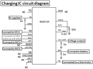
I am experiencing the following issues with a circuit using the BQ25122:
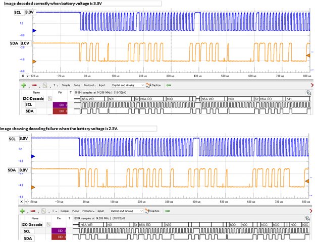
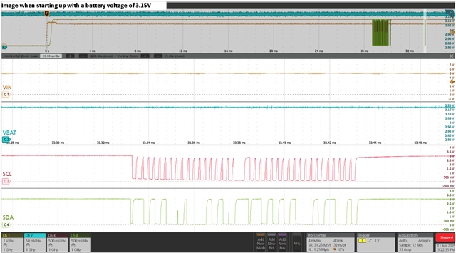
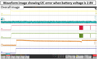
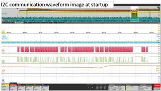
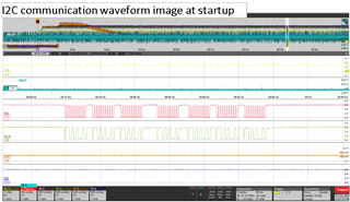
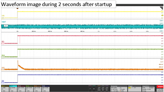
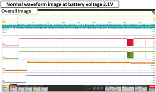
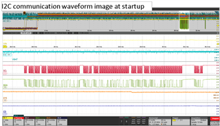
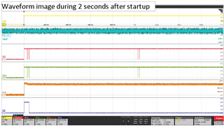
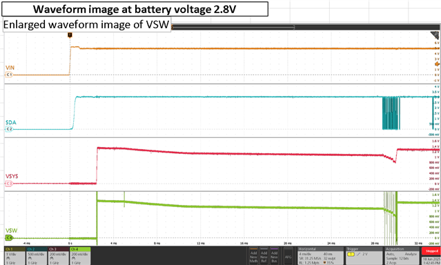
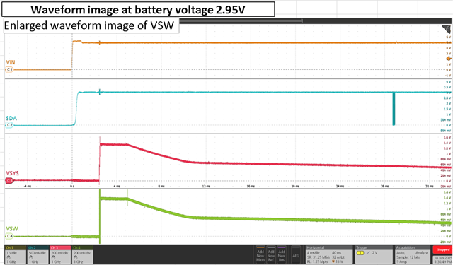
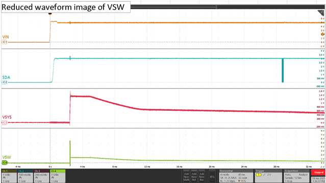
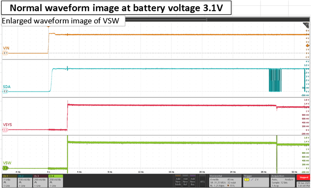
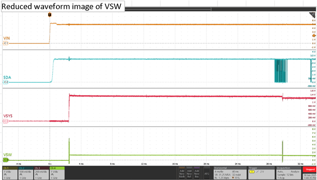
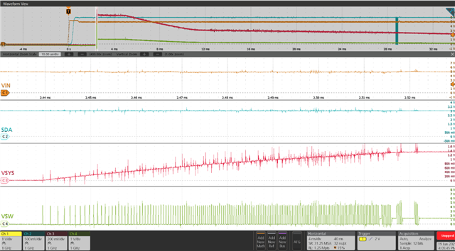
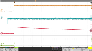
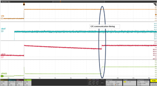
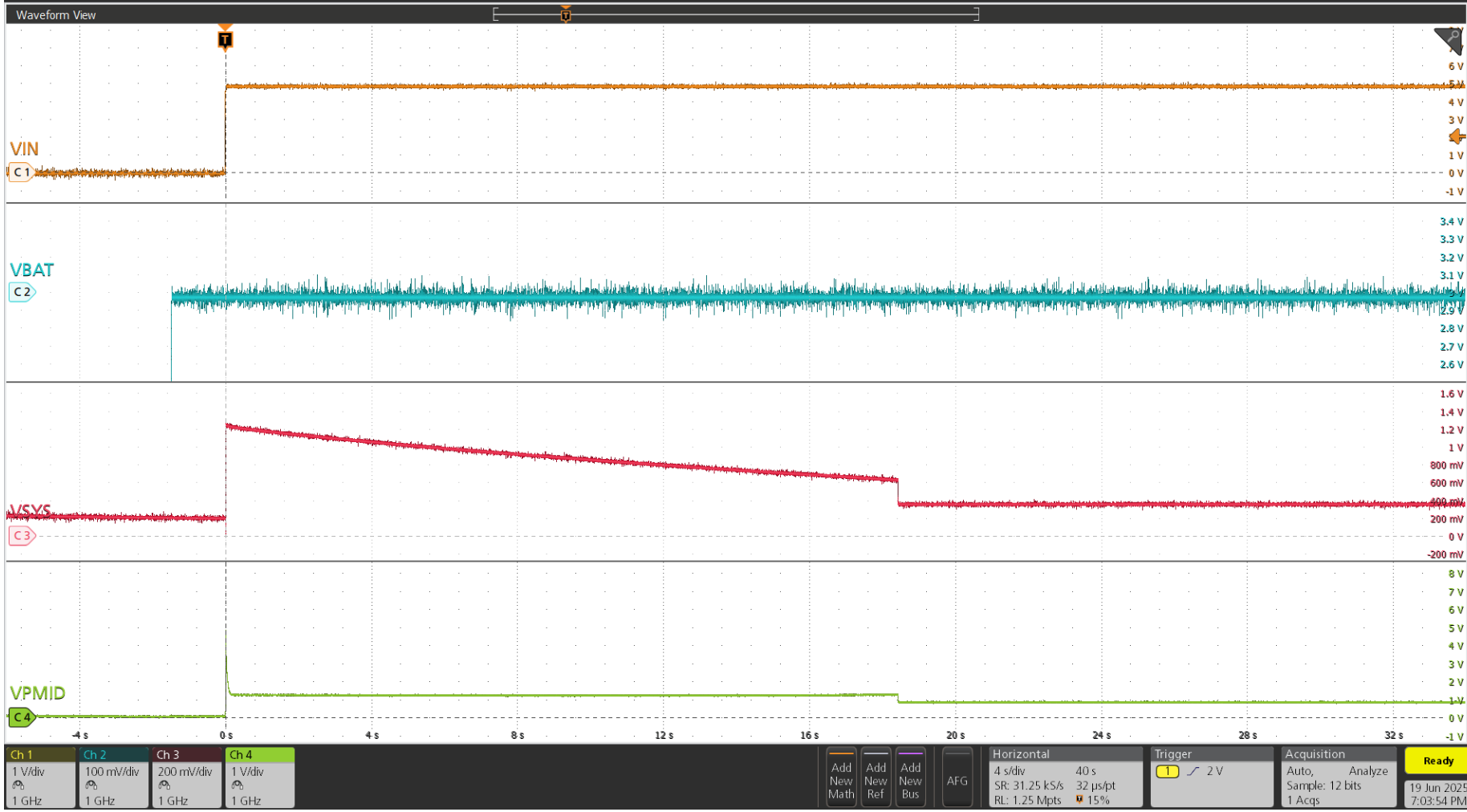
- When the battery voltage (VBAT) falls below BATUVLO (approx. 3.0V), the physical I2C waveforms can still be observed using an analyzer such as Analog Discovery, but I2C decoding fails or becomes unstable.
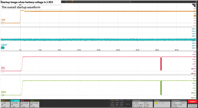
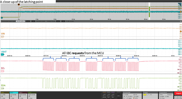
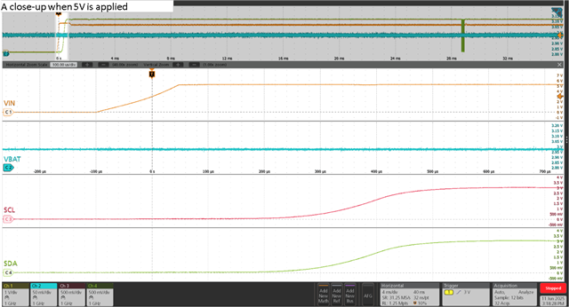
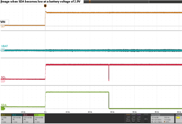
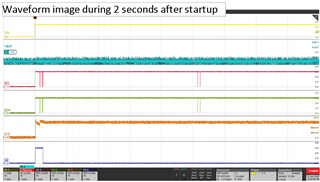
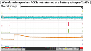
- Additionally, when VBAT is around 2.9V and 5V is applied to the IN pin, the I2C SDA line sometimes becomes latched at High or Low and does not respond.
Could you please advise on:
- The reasons why I2C communication becomes unstable below BATUVLO,
- And the mechanism by which SDA may become latched High or Low when 5V is applied while VBAT is low?
Any insights regarding the internal behavior of the device in this situation would be greatly appreciated.
Thank you very much.