This thread has been locked.

If you have a related question, please click the "Ask a related question" button in the top right corner. The newly created question will be automatically linked to this question.

TPS552892: TPS552892 design review

Part Number: TPS552892
Other Parts Discussed in Thread: TINA-TI

Tool/software:

Hi sir,

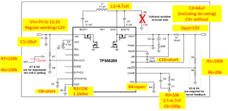
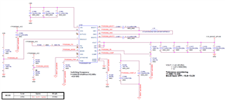
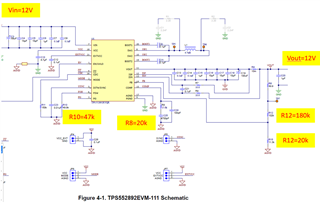
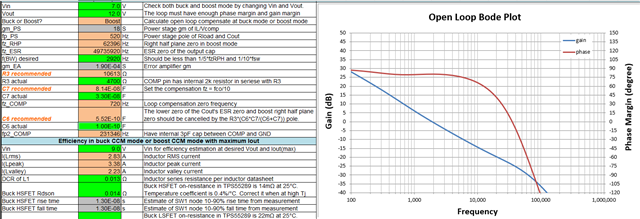
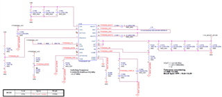
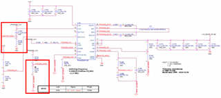
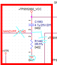
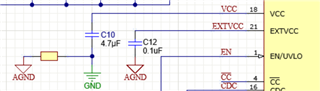
I selected TPS552892 to implement a buck-boost power supply.

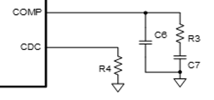
Base on the excel design sheet from TI official website, I have designed a set of parameters. 

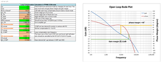
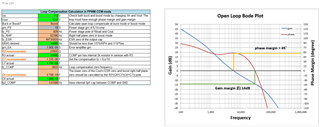
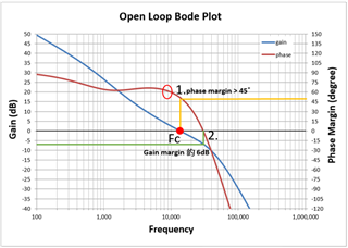
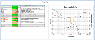
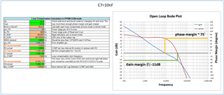
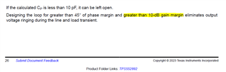
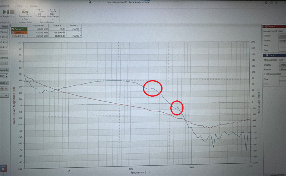
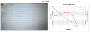
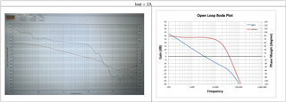
Could you please help check  if there are any issues,especially regrading the feedback response stability?

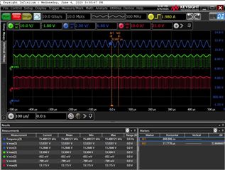
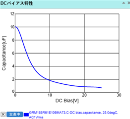
The bode plot is attached for your review and reference.

Thank you !!

Parameters:

Fsw=1.2MHz

Vin range 7V to 13.2V

Vout = 12V

delta Iout=100mA to 2A

  • Hi Danny,

    Thank you for using e2e forum.

    Our experts for this device is out of office. Please expect a response next week. Thank you for your patience.

    Best regards,

    Mounika

  • Hi Danny,

    1. For TPS552892 which is non-I2C version, the SCL and SDA pins are changed to PG and CC pins.

    2. MODE pin needs to connect with VCC or AGND to select FPWM or PFM mode.

    3. Check the effective capacitance of VCC cap is larger than 2.0uF at 5.2Vdc bias voltage.

    4. Recommend to change C7 from 4.7nF to 10nF.

    5. ISP and ISN need to connect to Vout directly if output sense resistor R1 is short.

    6. Follow the layout guidelines.

    7510.TPS55289 Layout Guide line.pdf

    BRs,

    Bryce

  • Hi Bryce,

    thanks for your reply.

    This is my original schematic design.

    As this schematic, the setting of parameter is followed document TPS552892EVM-111 EVM user guide.

    Abnormal oscillations occurred in the output and inductor current when there was a load transient variation(150mA/100ns).

    The waveform as below picture (blue=Vout ; yellow=IL ; green=SW1 ' Red=SW2)

    I tried to duplicate this issue form TPS552892EVM-111, I modify the resistor(R8) form 15k ohm to 20k ohm and remove electrolytic capacitor(C19).

    The same issue can still be observed when the EVM power on(without loading).Waveform as blew

    Question:

    1. Does the electrolytic can't remove ?

    2. In the abnormal waveform, the Vout shows an oscillation close to 25kHz,which is also present on the EVM even without loading.

    Does this be internal noise or digital circuit from IC feedback ?

    3. To ensure power supply stability,which parameter  should I consider ?

    For example:

    a. crossover frequency VS FLC

    b. phase margin

    c. gain margin

    d. Quality Factor

    e. damping

    Do these parameter have standard definitions. 

  • Hi Danny,

    From the waveform, it shows the loop is unstable.

    1. The electrolytic cap can be removed, but the COMP parameters need to be redesigned according to the new output capacitors.

    2. No, the oscillation is due to unstable loop, not from IC internal circuits.

    3. To validate the  loop stability, phase margin and gain margin is needed to be validated. Recommend PM>45deg and GM<-8dB. The cross frequency is the reflection of  loop response, higher cross frequency, faster loop response. But with higher cross frequency, the PM and GM may be inadequate. So there is a balance for that. 

    BRs,

    Bryce

  • Hi Bryce,

    1.OK,thanks !!

    2.The same frequency oscillation appears on both the system and the EVM. Base on your experience, Is there any possible relation between them?

    3.Is requirement of PM>45 deg and GM <-8dB defined by an official specification, or is it based on design experience?

    3-1.In original design, the gain margin is approximately -6 dB and PM > 45 deg,which is close to your specified -8 dB.Could this indicate a risk of system unstable? 

    3-2.I have made adjustments a setting of parameter and confirm with you before.

    You recommended changing C7 from 4.7nF to 10nF,does this result have any problems that's PM>60 deg.

    Other references suggest that 45 to 60  deg is the optimal range.

    May I ask the reason for recommending the change of C7 to 10nF?


    4.Would there be any stability concerns if crossover frequency(Fc) is designed to be close to the resonant frequency(FLC)?

    Do you have any suggestions regarding the relationship between Fc and FLC?

    Vin=12V/Vout=12V/Cout=64uF/L=4.7uH/Iout=0.2 to 1.5A

    FLC = 9.1kHz

    TPS55289-CALCULATION-TOOL_0610調整參數_V1_L4R7.xlsx

  • Hi Danny,

    Please see my replies below.

    2.The same frequency oscillation appears on both the system and the EVM. Base on your experience, Is there any possible relation between them?

    3.Is requirement of PM>45 deg and GM <-8dB defined by an official specification, or is it based on design experience?

    3-1.In original design, the gain margin is approximately -6 dB and PM > 45 deg,which is close to your specified -8 dB.Could this indicate a risk of system unstable? 

    2. No relation between them, the oscillation frequency is also the cross frequency but with no margin, so when there is a distortion with that frequency, the system is not convergent, then it shows the oscillation on the waveforms.

    3. The PM>45deg and GM<-8dB is from engineering experience. 

    3-1. No, the -8dB is the engineering experience value which means the system is robust enough to face distortions. And you also need to check if the values in the excel tool is corresponding to the bench values, for example, the dc bias effect of MLCCs should also be considered.

    3-2. Changing 4.7nF to 10nF, so the phase margin is higher.

    4. No, the FLC is caused unstable system loop. And cross frequency should be designed less than 1/5-1/10 RHPZ at boost mode, and also 1/5-1/10 switching frequency.

    5. Below is modified excel file with the schematic shared before.

    3660.TPS55289-CALCULATION-TOOL_0610調整參數_V1_L4R7.xlsx

    BRs,

    Bryce

  • Hi Bryce,

    I sincerely appreciate your time and patience in answering my questions.

    The system operating  range is 0.2A to 2A.

    Today I used the Bode-100 to measure the frequency response.

    I have two sets of measurement result,please help review and provide your comments. 

    Q1. which one is better suitable for actual application?

    Q2.Is it necessary to ensure that the PM>45 deg and GM<-8 dB are cover the full loading range? 

    Q3.Base on your experience, what is generally considered an acceptable range for PM?

    etc. 45 deg to 90 deg ? 

    please reference blew symbol component ref.name

    1. R3=10k , C7=10nF , C6=100pF

    (You recommend value)

    Iout=200mA

    Iout=2A

    2.R3=9.1k , C7=22nF , C6=100pF

    Iout=200mA

    Iout=2A

  • Hi Danny,

    Q1: From the results, with 10k+10nF, 100pF, the PM is less than 45deg and GM larger than -6dB which is not preferred. The results of 9.1k+22nF, 100pF looks better. 

    Q2: Yes, the PM and GM value criteria need to cover all operating profile. From Min Vin to Max Vin and light load to full load. The GM criteria can be loose to -6dB.

    Q3: Generally, we would consider 45deg or 60deg as acceptable range. 90deg is good but will need to sacrifice the cross frequency.

    BRs,

    Bryce

  • Hi Bryce,

    I noticed that the TPS552892 datasheet specifies a GM requirement of greater than -10dB.

    I want to reconfirm some key point about loop stability design.

    1. Phase Margin range is 45deg or 60deg as acceptable range.

    2. Gain Margin requirement of greater than -10dB,but must not less than -6dB.

    From Min Vin to Max Vin and light load to full load. The GM criteria can be loose to -6dB.

    3.At boost mode, cross frequency should be designed less than 1/5-1/10 RHPZ , and also 1/5-1/10 switching frequency.

    Please let me know if there have any other key requirement we should consider to ensure loop stability.Thank you very much.

  • Hi Danny,

    1. Phase margin 45deg is acceptable, 60deg is better with higher margin.

    2. Gain margin smaller than -6dB is acceptable, -10dB is better.

    3. Correct.

    For loop stability, the key specs are cross frequency, phase margin and gain margin.

    BRs,

    Bryce

  • Hi Bryce,

    As your reply item 1, "1. Phase margin 45deg is acceptable, 60deg is better with higher margin."

    Below is our bode test in real case, some condtion phase margin is over 80deg.

    Is it too high for phase margin? And it will impact transient respone?

    Note. We use R3=4.7k, C7=33nF, C6=100p.

  • Hi Bryce,

    Another question from customer, phase line(blue one) have some glitch, is it impact by Rcomp or Ccomp?

    Is it impact the buck-boost performance? Thanks!

    Jeff

  • Hi Jeff,

    80deg phase margin is ok, it is not a problem with high phase margin. If the phase margin is too large, it usually means the cross frequency could be increased to achieve faster loop response. It is a balance between cross frequency and phase margin.

    The glitch is caused by test, not from the control loop. It will not affect the loop performance.

    BRs,

    Bryce

  • Hi Bryce,

    Following Jeff's information,the comp circuit design is R3=4.7k, C7=33nF, C6=100p.

    Could you help explain the reason for the bode plot difference between the measured and estimated(Excel) ?

    Does there have any important key factor I missed?

    The inductor and Cout value were measured by LCR meter.

    L=4.55uH, Cout=95uF(at 12V)

    Here are the measured and estimated waveform, 1. Iout=0.2A. 2. Iout=2A.  

    Iout=0.2A

    Iout=2A

    Considering the significant difference between measured and estimated waveforms, what approach would you recommend for evaluating future designs or applications?

    TPS55289-CALCULATION-TOOL_0623.xlsx

  • Hi Bryce,

    Does the TPS552892 have a TINA-TI model for simulation?

    If TINA-TI model is not available,are there any other simulation tools recommended for evaluating during design stage?

  • Hi Danny,

    You can find Pspice model from ti.com.

    Regards,

    Mulin

  • Hi Bryce,

    Do you have any update on this? This is an urgent case.Please kindly respond ASAP.

    Thanks !!

  • Hi Danny,

    Bryce is OoO today, please expect a late reply.

    Regards,

    Mulin

  • Hi Danny,

    Sorry for the late reply, I was on business traveling this week.

    Can you share the final schematic you tested the bode plot with? And also share the input, output conditions, and the part number of output capacitors?

    We don't have TINA-TI model for recently released device, and the PSpice model is more recommended by TI in recent years. Below is the download link of the PSpice for TI model, and you can also find it in the Product Page at ti.com

    https://www.ti.com/lit/zip/slvme05

    BRs,

    Bryce

  • Hi Bryce,

    The schematic as below,Cout + Cin(next stage Efuse)  

    Part number of capacitor

    1. Cout: 0805/22uF:0805X226M250CT (Walsin)

    2. Cin(E-fuse): 0603/10uF:0603X106M250CT (Walsin)

    Vin range 7V ~ 13.2V , general Vin=12V

    Vout = 12V

    delta Iout=200mA ~ 2A , from idle to working 

    Bode plot

    Vin12V 200mA

    Vin12V 1A

    Vin12V 2A

    Vin10V 2A

    Vin13.2V 2A

  • Hi Danny,

    Compared the schematic with the parameters you filled in the Calculation Tool, the main difference is the output capacitance. Since I can't find the effective capacitance of the output caps you used, so I used the similar value of Murata cap with same rated capacitance/package size/voltage rating to estimate the effective capacitance. And for the 22uF/25V/0805 cap, the effective capacitance is about 3.8uF at 12V dc bias voltage each. For the 10uF/25V/0603 cap, I used GRM188R61E106MA73 as reference, the effective capacitance is about 1.5uF at 12Vdc bias voltage each.

    Below is the Calculation Tool I used with the estimated output capacitance. The result is similar to your test result, but may have minor difference due to capacitance/inductance variance and IC variation.

    TPS552892 Design Calculation V1.0_0627.xlsx

    About the schematic:

    1. Recommend to connect the VCC ground with PGND. And connect PGND with AGND through net tie at VCC cap ground.

    2. Connect the R1434 ground with AGND.

    3. Follow the layout guidelines and send to us for review when finished.

    BRs,

    Bryce

  • Hi Bryce,

    Thanks for your suggestion!!

    The modify schematic as below,is this correct?   

  • Hi Danny,

    Recommend to change the GND of VCC cap to PGND as below.

    BRs,

    Bryce

  • Hi Bryce,

    Got it. Thank you for your help !!!

  • Hi Danny,

    Thanks, I will close this thread, you can reply it here if any more questions, then the thread can be opened again.

    BRs,

    Bryce