


Other Parts Discussed in Thread: LM74800-Q1
Tool/software:
Hello everyone,
We currently use the LM74800-Q1 IC as an ideal diode driver for an application. This driver is used in conjunction with an ISCH42N04LM7ATMA1 power MOSFET (extremely low Rdson).
This pair is used to connect to 2 power sources to a main bus powering some electronics and motors. The IC + MOSFET is configured in a common drain configuration, with only the ideal diode side being used (no use of HGATE). The idea being that if a power source fails, no back current flows to it. Furthermore, when our motors are braking (active braking), as the voltage rises on the main output bus, we protect the power source, thanks to the ideal diodes. The sources have their own OVLO, but we want to avoid that, hence the ideal diode.
Here is the schematic of the ideal diode part in our design (2x on the board, one for each power source).

Note that the +24V side has some bulk capacitance (about 670uF). The output is connected to the electronics and motors (also some capacitance, a lot near the motors). An energy dump circuit is also present, it will trigger when the output bus voltage goes too high during braking and will dump the excess energy in some resistors.
We tested this circuit with a setup with a simple single electrical motor running with a propeller to generate some torque. The motor goes from positive rotation to negative very fast.
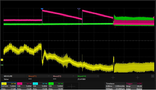
The oscilloscope capture above has the following curves: Yellow: current to/from motor. Blue: VGate power source 1. Pink: VGate power source 2. Green: Output bus voltage (common drain).
What we see is a braking of a motor. For a very brief moment at the beginning, reverse current is detected (Vgate was regulated at a low enough level during steady state, detection is fast). Then current is back up and Vgate is driven super high, it then drops linearly until the next spike. But during this low Vgate linear down regulation, current starts to flow back. The problem is that it will start to feed the bulk capacitors as the rail goes up. Now we have Anode and Cathode going up and the reverse current protection is not able to work properly.
To me it looks like the linear regulation is too soft/ slow. It means that if we go from 0A, then a current surge happens, the Gate will go as high as possible to get the 10mV drop out (which is good). But the if the current then reverse or falls down fast enough, the regulation doesn't follow quickly enough, essentially keeping a low Rdson, making the back current detection harder and the protection delayed (Vgate going to Vs to open the circuit)
So my questions are as follows:
Did I understand this scenario properly ?
Is it normal for the regulation to be going down on Vgate that slowly ?
What would be the best approach to make the system more responsive ?
Would it be better to move the bulk capacitance on the cathode side instead of the anode side ?
Thanks in advance for your help. don't hesitate to ask me for clarifications or more details on this case.
Best regards,
Marc
