Tool/software:
I have implemented the buck/boost design as defined by the webbench tool (report attached) for a supply input of 6-36V and output of 12V at a maximum of 0.5A. Powering the design with various inputs in that range with no load and 0.1A load, the output voltage is always 0.7V instead of 12V.
I don't see anything obviously wrong. Could the lower load be causing instability? And are there any suggestions on alternate part values to allow the current PCB to function?
Thank you in advance.
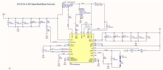
My schematic is:
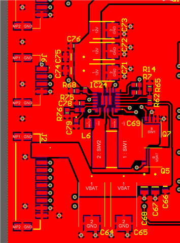
Layout top:
Layout Bottom:
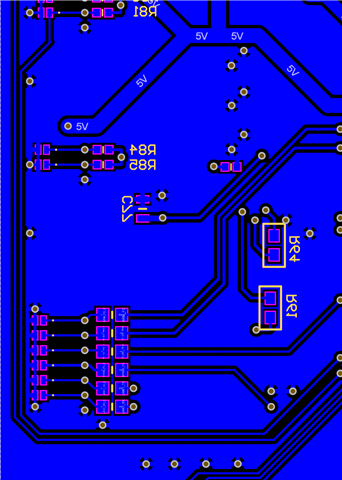
and have internal solid ground plane.
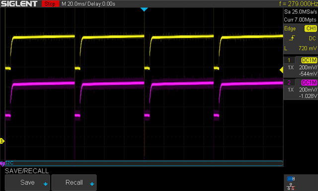
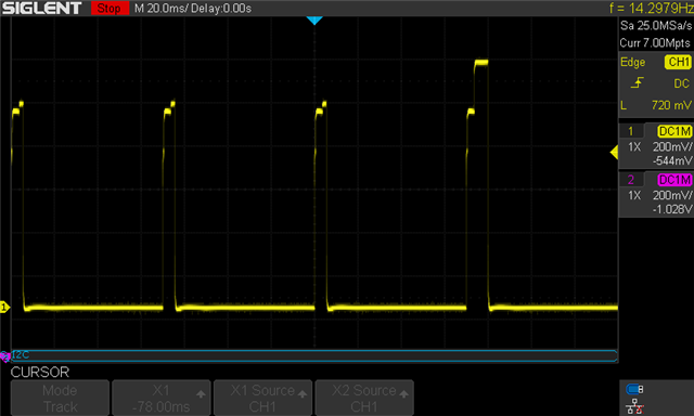
Testing the design with 17V input:
EN/UVLO is 12.2V
and probed the following signals
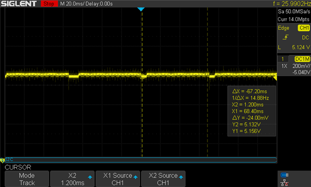
SW1 (yellow) and SW2 (purple):
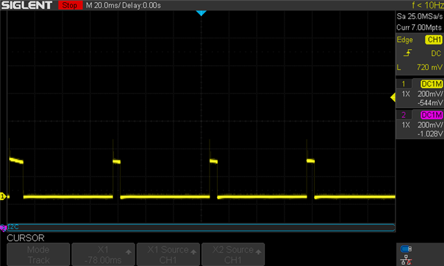
COMP:
ILM: