Tool/software:
Hi TI members,
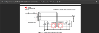
I am following the circuit CKT 1 from the TI manual 1 "Configurations of Secondary Rectifier Circuit using UCC24624" for the efficiency improvement for my LLC Converter.
CKT 1:
If the Vout can go higher and also to avoid DCM rings, some resistors(see RED Circle below) are used as mentioned in the TI manual: 2 of UCC24624, as given below,
"UCC24624 Dual-Channel Synchronous Rectifier Controller for LLC Resonant Converters"

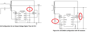
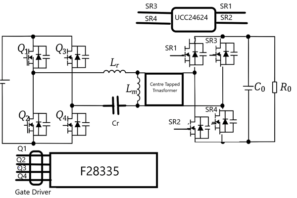
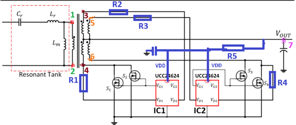
Considering all the effects, I designed the schematic shown below, based on TI manual 1 above circuit CKT 1 using 4 Resistors R1,R2,R3 & R4 are included to avoid DCM rings. The Vout can go higher; therefore, another R5 is used from the Vout to VDD of both ICs (UCC24624). All resistors are set to 1K ohm as recommended by the TI datasheet of UCC24624 for approaching the requirement.
The schematic with all Node Points is shown below. Here, I designed the transformer with a turns ratio (2:1) along with center-tapped windings. The MOSFETs are used having low RDS (5m Ohms) and low charge recovery (Qrr = low). During operation, I see the results on the Oscilloscope with waveforms at different nodes from the UCC24624. Please see the Schematic below
Schematic:
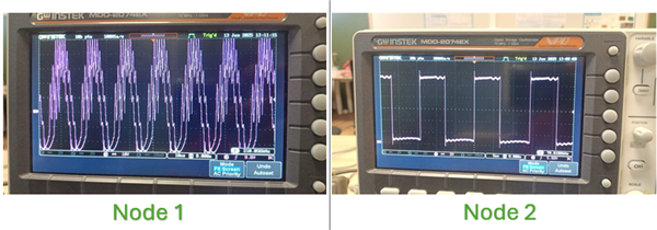
Primary Side Node 1 & Node 2 Resonant Tank Outputs followed by Full Bridge Inverter (Square Wave Signals):
Node 1 & Node 2:
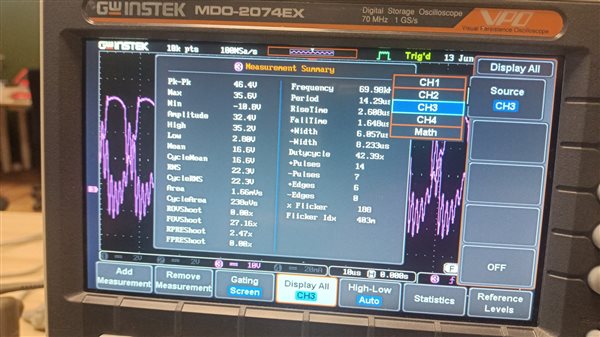
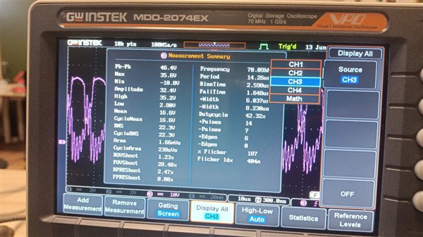
Secondary 1: Node 3 & Node 4(Inverted) Outputs having both RMS values 22Volt at 70Khz (near Resonance pk 60Khz):
Node 3
Node 4

Secondary 2: Node 5 and Node 6(Inverted) Outputs having both RMS values 22Volt at 70Khz (near Resonance pk 60Khz):
Node 5
Node 6
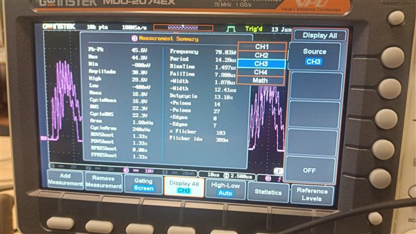
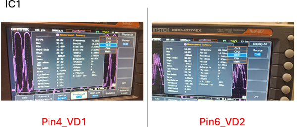
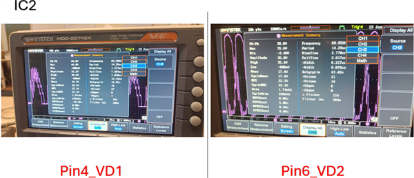
Now, the Drain voltage sensing (VD1,VD2,VD3,VD4) of Synch Rect Controller IC1 & IC2 Just after the Resistors R1,R2,R3,R4 (Same Outputs having both RMS values 22Volt at 70Khz (near Resonance pk 60Khz) :
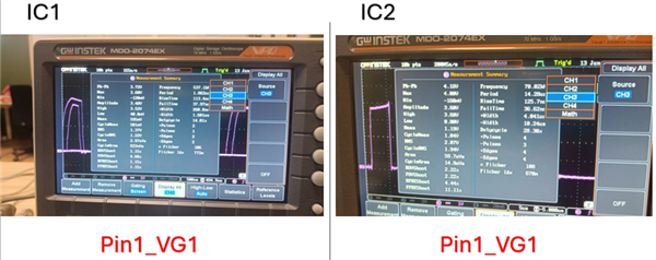
Since no VG2 connection in the schematic, only the Gate voltage VG1 of the MOSFETS of Synch Rect Controller IC1 & IC2 are the Pulse signals shown below. Here, both gate voltages of IC1 and IC2 are VG1 = 3.7Vpk-pk, VG1 = 4Vpk-pk, respectively. (not completely synchronized or matched pulses).
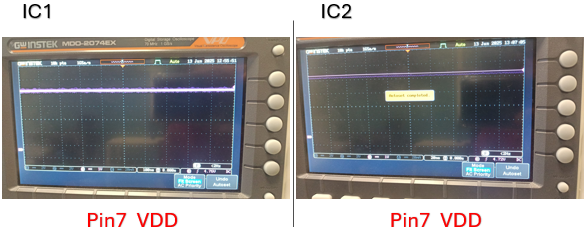
VDD (Pin 7) of Synch Rect Controller IC1 & IC2 are at DC voltage = 4.7V each as shown below:
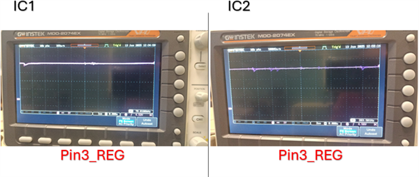
The Regulator REG (Pin 7) of Synch Rect Controller IC1 & IC2 stays at DC voltage = 4.5V each as shown below:
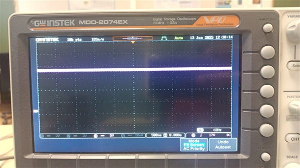
The final output we get at Vout at Node 7 (DC Volatge) Vout = 17V at the LLC Output at 70Khz (near resonance peak 60Khz).
With all these above measurements images, I would like you to guide me in identifying the correct operation of Synchronous controllers in the above designed Schematic and explain to me why I am losing EFFICIENCY after some calculations of Pin and Pout instead of improving it by using Synchronous Rectifier Controller.
Please suggest accordingly.
Thanks
Regards
Arsalan