This thread has been locked.

If you have a related question, please click the "Ask a related question" button in the top right corner. The newly created question will be automatically linked to this question.

BQ24133EVM-715-15V: Power Path No Longer Correct

Part Number: BQ24133EVM-715-15V
Other Parts Discussed in Thread: BQ24133, EV2400, BQSTUDIO

Tool/software:

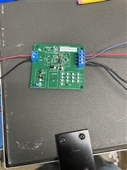
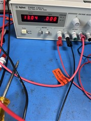
I have the BQ24133EVM-715-15V and am supplying 16V in, following the user guide "bq24133 User's Guide" I got it working perfectly but after 2 uses of only running it for about 20min total the VSYS now reads 2.0V when a battery is not connected and when a battery is connected it reads the batteries voltage when measuring with a multimeter from a gnd pin and VSYS.  I thought maybe somehow I damaged the device so I purchased a second eval board and have the exact same issue the board works fine and out of nowhere stops working. It is as if the path from Vin to VSYS is broken but I cannot figure out why it is reading 2.0V at all. Could something be wrong with the fets? Anyway to prevent or fix this issue? 

  • Hi Terence,

    Is the ACDRV pin outputting the drive voltage for the FETs and the FETs are the not turning on?  If so, then the FETs are damaged but the IC is okay.  The gate to source abs max voltage for those FETs is shown below.  If you are hot plugging the 16V input source, I'm wondering if a voltage spike is damaging the FETs.  

    If not, what is the voltage on the OVPSET pin? If near 1.6V, then the part thinks the input voltage is too high and is not turning on the FETs.  Can you lower your input source and try again?  If you bypass (short across) the FETs, does this charge function as expected?

    Regards,

    Jeff

  • Thank you for the fast reply! 

    Here is the reading for each test on the PCB when applying 16V 

    TP 7: 0.1V

    TP8: 0V

    TP9: 0V

    TP10: 0.4V

    TP11: 1.2V

    TP12: 1.9V

    TP13: 1.2V

    TP14: 1.2V

    TP15: 15.7V

    TP16: 3.22V

    TP17: 6V

    TP18: 0V

    TP19: N/A

    TP20: 0

    I am going to order replacement components for Q2, Q3, Q4, and U1. I will update after swapping out components and seeing which one is the issue. I do not recall hot plugging the device but if that is the issue would adding more caps to the Vin be a viable solution?

  • Hi Terence,

    I am confused here.  OVPSET is zero which means there is no input voltage applied.  ACDRV is 0V so the input FETS are off.  BATDRV is 0 so battery FET is on.  But AVCC = 15.7V which must be coming from the battery?   BQ24133 is a 3S charger with max recommended operating voltage of 13.5V on the output and 20V abs max.  The battery FET Q4 CSD25302Q2  max gate to source voltage is +/-8V and you are apply twice that.

    Regards,

    Jeff   

  • I am not sure what is going on either. But it does seem to be the FETs which are damaged. 

    I have shorted the source and drain of both Q2 and Q3. I have also attached a picture of my setup. There is no battery or load connected during the time of taking measurements.

    Here is the reading for each test point on the PCB after shorting Q2 and Q3 source and drain while applying 13V

    TP 7: 6.2V

    TP8: 12.68V

    TP9: 0

    TP10:0

    TP11: 0

    TP12: 0

    TP13: 0

    TP14: 0

    TP15:12.94V

    TP16: 0

    TP17:0

    TP18: 13V

    TP19: 11.4V

    TP20: 0

  • Hi Terence,

    OVPSET at TP9 is the mid point of resistor divider from VIN.  Why is it zero? If it is zero, I'm not certain what the IC will do since AVCC.  

    Regards,

    Jeff

  • Hello Jeff,

    I replaced Q2 and Q3, and the PCB is now working as expected. I just completed going through the bq24133 User's Guide, and everything checked out well.

    I have two final questions:

    1. The user guide recommends using a 16V input for the evaluation version I have, according to the "002" configuration notes. Section 1.5 lists the input voltage range as 6V to 18V. However, when I supply 6V or even slightly higher voltages VSYS does not output correctly, as if U1 isn't turning on at all. Once I increase the input to 12V or higher, everything works as expected. I understand that the OVP threshold is set by the R6/R9 voltage divider, but what sets the undervoltage threshold for the input?

    2. Lastly, is there anything you would recommend for a new design to help prevent the failure I encountered earlier?

  • Hi Terence,

    Regarding 1, the OVPSET resistors also set UV threshold.  The reference for OV is 1.6V and the reference for UV is 0.5V.  So if OV is set for 17V, UV is 17/1.6*0.5 = 5.3V.

    Regarding 2, I don't think we determined the exact cause of failure, did we?  I think the gate drive for the battery FET may still be an issue.

    Regards,

    Jeff

  • Hello Jeff,

    Thanks for the clarification regarding the UV threshold.

    Also, I forgot to mention earlier that I replaced Q4 (the battery FET), so that should no longer be a concern. Based on my latest tests, it looks like all FETs are now switching correctly:

    • With only VIN applied at 16V, VSYS = 16V

    • With only VBATT (8.2V, 2-cell pack) connected, VSYS = 8.2V

    • With VBATT connected and VIN applied, VSYS correctly switches to VIN (16V), and the battery begins charging as expected

    I’m also monitoring the system using bqStudio with the EV2400, and everything appears to be operating normally now.

    Let me know if there’s anything else you’d recommend checking!

    Best regards,
    Terence

  • Hi Terence, 

    If its working and battery FET gate drive is within the FET's limits, I don't see any other issues.

    Regards,

    Jeff