Tool/software:
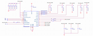
Hello expert, I would like to confirm the default output voltage of each power supply for the PTPS6521402VAFR PMIC chip. Thank you!
Original question:

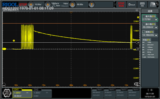
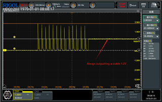
TPS65214: I want to know the reason and solution for this inability to output normally
Tool/software:
Hello expert, I would like to confirm the default output voltage of each power supply for the PTPS6521402VAFR PMIC chip. Thank you!