This thread has been locked.

If you have a related question, please click the "Ask a related question" button in the top right corner. The newly created question will be automatically linked to this question.

TPS3701: VPU Supply Options – Using a Resistor Divider

Part Number: TPS3701

Tool/software:

Hello all,

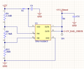
I’m currently using two TPS3701 (TPS3701DDCT) devices to monitor two separate voltage rails: +15V and -15V. These components, along with their supporting circuitry, are placed on a dedicated “Power Rail PCB,” which connects to a main control board.

Application Context:
The goal is to detect when either rail deviates beyond ±10% of its nominal value. If such a deviation occurs, the TPS3701 outputs a logic signal that is sent back to the control board.

This is the second revision of this design. In the earlier version, I used optocouplers instead of the TPS3701, with a 3.3V supply (for logic output pull-up) provided by the control board. However, that 3.3V line was quite noisy, resulting in unstable and unreliable logic signals from the optocouplers.

To improve reliability, I’ve switched to the TPS3701 in this revision.

My Question:
Given that the 3.3V supply from the control board might still be noisy, would it be viable (or advisable) to generate a cleaner 3.3V locally by using the +15V rail (already present on the Power Rail PCB) and stepping it down with a resistor divider for use as the VPU (pull-up voltage) for the TPS3701?

I’d appreciate any guidance or recommendations—especially regarding any risks or best practices when using a resistor divider for this purpose.

Best regards,
Kosta Kotsis

  • Our team will respond in next 24 hours. Thanks.

  • Hi Kosta,

    Are you able to share a schematic for this design?

    Jesse 

  • Hello Jesse,

    Below I am attaching pictures of the schematic for both the variants I have mentioned above:

    Variant A – Using External 3.3 V Rail

    In this version, the 3.3 V rail coming from the control board is used directly as the VPU for the TPS3701 on the Power Rail PCB.


    Variant B – No 3.3 V Rail, VPU Derived from +15 V

    Here, the 3.3 V rail is completely removed. Instead, VPU is derived locally from the +15 V rail (generated by a local SMPS on the Power Rail PCB) using a resistor divider and a Zener diode (Vz = 3.3 V) to clamp the logic output voltage to 3.3 V. This approach ensures the logic level remains compatible with 3.3 V digital inputs, even if the +15 V rail varies above nominal.


    Question Regarding Variant B – Monitoring Negative Rail

    One of the TPS3701s (U1) is used to monitor a –15 V rail. Should the output stage of U1 be implemented in the same way as U2, which monitors the +15 V rail?

    According to TI documentation, when monitoring a negative voltage, it's recommended to place a diode with low forward voltage between the logic output and GND to ensure the output reliably pulls low. However, I'm unsure how this affects logic output behavior if the +15 V rail rises significantly above nominal, especially in the absence of a Zener clamp on VPU in this case.

    Would this risk exposing the input of a downstream logic device to voltages above its safe operating range, or causing any other issues?

    Any insights or recommendations you can share would be greatly appreciated.

    Best regards,
    Kosta Kotsis

  • Hi Kosta,

    Sorry for the delay, my answer is below.

    One of the TPS3701s (U1) is used to monitor a –15 V rail. Should the output stage of U1 be implemented in the same way as U2, which monitors the +15 V rail?

    When U1 asserts, the outputs are going to be pulled down to -15V, so my question is, where ever the -15V_RAIL_CHECK signal is going, can it take the negative voltage. 

    According to TI documentation, when monitoring a negative voltage, it's recommended to place a diode with low forward voltage between the logic output and GND to ensure the output reliably pulls low. However, I'm unsure how this affects logic output behavior if the +15 V rail rises significantly above nominal, especially in the absence of a Zener clamp on VPU in this case.

    This configuration is advised for the +15V. The diode is typically not necessary when monitoring positive voltage unless there are concerns of the current flipping. 

    Would this risk exposing the input of a downstream logic device to voltages above its safe operating range, or causing any other issues?

    With the schematic above, there should not be any risk of exposing the input of a downstream logic device to the up stream voltages. For the negative voltage monitoring it will depends on how you would process the output. I would highly recommend phase shifting the negative voltage rail as outlined below.

    https://www.ti.com/seclit/eb/slyy167/slyy167.pdf?ts=1752105801212&ref_url=https%253A%252F%252Flogin.ti.com%252F

    Jesse